Wafer Backside Thinning Service Market Insights 2026, Analysis and Forecast to 2031
- Single User License (1 Users) $ 3,500
- Team License (2~5 Users) $ 4,500
- Corporate License (>5 Users) $ 5,500
The semiconductor manufacturing landscape is currently navigating a pivotal transition from planar scaling to three-dimensional integration, a shift that has fundamentally elevated the strategic importance of the wafer backside thinning service market. As the industry confronts the physical and economic barriers of Moore Law, the ability to vertically stack integrated circuits and minimize package profiles has become a prerequisite for performance advancement. Wafer backside thinning, a process that reduces the thickness of a semiconductor substrate to a fraction of a human hair, is no longer merely a finishing step for smart cards or power discretes; it has evolved into a critical enabling technology for high-performance computing, 5G communication, and electric mobility.
The essence of this market lies in the precision removal of bulk material from the backside of a processed wafer. This process serves multiple critical functions: it improves thermal dissipation by reducing the thermal resistance path, it enables the exposure of Through-Silicon Vias or TSVs for vertical interconnects in 3D-IC packaging, and it significantly reduces the electrical resistance in vertical power devices. The technical complexity of thinning has increased exponentially as wafer diameters have shifted to 300mm and thicknesses have decreased to below 50 microns. At these dimensions, silicon behaves less like a rigid plate and more like a flexible membrane, introducing severe challenges related to warpage, handling, and stress management. Consequently, the market for thinning services has bifurcated into high-volume, standardized processing for consumer electronics and high-value, specialized processing for advanced packaging and heterogeneous integration.
Based on an assessment of the current industrial trajectory and the increasing adoption of advanced packaging technologies such as Fan-Out Wafer-Level Packaging and System-in-Package, the global wafer backside thinning service market size for the year 2025 is estimated to be in the range of 1.8 billion to 3.1 billion USD. The market is projected to expand at a Compound Annual Growth Rate or CAGR estimated between 7.2 percent and 10.5 percent over the subsequent forecast period. This robust growth is primarily driven by the burgeoning demand for AI servers requiring High Bandwidth Memory, which relies heavily on stacking thinned memory dies, and the electrification of the automotive sector, which demands ultra-thin power semiconductors for efficiency.
Recent Industry Developments and Strategic Realignment
The year 2025 has witnessed significant strategic realignments within the semiconductor supply chain, characterized by consolidation in the high-reliability sector and aggressive capacity expansion in the advanced packaging domain. These developments underscore the critical nature of back-end processing services.
On January 15, 2025, Micross Components, Inc., a premier provider of high-reliability microelectronic product and service solutions tailored for aerospace, defense, space, medical, and industrial sectors, finalized the acquisition of Integra Technologies. Integra Technologies, headquartered in Wichita, Kansas, is a specialist Outsourced Semiconductor Assembly and Test or OSAT provider focusing on post-processing for high-reliability applications. This acquisition is a significant milestone in the consolidation of the United States domestic supply chain. By absorbing Integra capabilities, Micross has reinforced its position as a leader in US-based OSAT services. The integration broadens the Micross portfolio, allowing it to offer a seamless, end-to-end solution that encompasses die preparation, thinning, and packaging for mission-critical electronics. This move is particularly relevant in the context of increasing geopolitical friction, as it strengthens the secure supply chain for defense and aerospace clients who require domestic, ITAR-compliant processing services.
Later in the year, on August 13, 2025, the ASE Group, recognized as the world leading OSAT provider, executed a bold expansion strategy to address the skyrocketing demand for advanced packaging. ASE acquired a facility from the GaAs foundry WIN Semiconductors, located in the Southern Taiwan Science Park in Kaohsiung. The transaction, valued at NT 6.5 billion, includes the plant and related infrastructure. This acquisition is a direct response to the capacity bottlenecks faced by the industry in high-end packaging, particularly for AI and high-performance computing chips. The facility is expected to be retrofitted to support advanced packaging workflows, including wafer bumping, thinning, and heterogeneous integration. This move highlights the intense pressure on top-tier OSATs to scale up their physical footprint and processing capabilities to support the manufacturing of complex, vertically stacked systems.
Value Chain and Industry Ecosystem Analysis
The value chain of the wafer backside thinning service market is a highly interdependent ecosystem that spans material science, precision machinery, and process engineering.
The upstream sector consists of equipment and consumable manufacturers. Companies like DISCO Corporation and AXUS Technology provide the fundamental machinery—grinders, polishers, and CMP systems. The performance of these tools defines the physical limits of the thinning process. Equally critical are the suppliers of consumables, such as grinding wheels, polishing pads, and protective tapes. The protective tape, or backgrinding tape, plays a vital role in protecting the active circuitry on the front side of the wafer during the aggressive mechanical grinding process. Innovation in tape technology, particularly in UV-curable tapes that allow for easy release without residue, is a key enabler for handling ultra-thin wafers.
The midstream sector is occupied by the service providers themselves. This segment is diverse, ranging from pure-play service bureaus like Syagrus Systems and Valley Design, which offer specialized, low-to-medium volume services, to massive OSATs like ASE and Winstek that perform thinning as an integrated part of a high-volume assembly line. There is also a segment of foundry-affiliated service providers, such as those within the Huahong Group ecosystem, that offer thinning as an extension of wafer fabrication.
The downstream sector comprises the end-users and integrators. This includes fabless design houses, IDMs (Integrated Device Manufacturers), and OEMs in consumer electronics and automotive sectors. The interaction between the service provider and the downstream user is becoming increasingly collaborative. For instance, in the manufacturing of Silicon Carbide power modules, the feedback loop between the thinning service provider and the device manufacturer is continuous to optimize the trade-off between wafer thickness (efficiency) and yield (breakage).
Process Types and Technology Trends
The market is segmented by the specific methodologies employed to reduce wafer thickness, each addressing different quality and throughput requirements.
● Grinding is the foundational process in the market and accounts for the largest share of throughput. It involves a two-step mechanical process: coarse grinding to remove the bulk of the silicon substrate rapidly, followed by fine grinding to achieve the near-final thickness and improve surface roughness. The trend in grinding is the migration toward in-feed grinding with extremely fine-grit wheels (up to #8000 mesh) to minimize the depth of the subsurface damage layer. However, mechanical grinding invariably leaves residual stress and micro-cracks in the crystal lattice, which must be addressed in subsequent steps.
● Etching is utilized primarily for stress relief and wafer strengthening. After mechanical grinding, the silicon lattice is damaged, significantly reducing the die fracture strength. Wet etching, using acid mixtures (typically spin-etched), removes this damaged layer without introducing new mechanical stress, effectively restoring the flexibility and strength of the wafer. This is critical for smart cards and flexible electronics. Dry etching, or plasma stress relief, is gaining traction for advanced nodes where wet chemistry might penetrate and damage the active device layers or bump structures. The trend is toward fully automated dry etching systems that can handle ultra-thin wafers without physical contact.
● Others includes Chemical Mechanical Polishing or CMP and hybrid finishing techniques. CMP is essential for 3D-IC applications involving Through-Silicon Vias. In these applications, the wafer must be thinned to reveal the copper vias buried within the silicon. CMP provides the global planarization necessary to expose these vias uniformly and prepare the surface for hybrid bonding. The demand for CMP services is growing faster than the overall market due to the proliferation of chiplet architectures and stacked memory.
Application Analysis and Market Segmentation
The demand for wafer thinning is heterogeneous, driven by distinct performance metrics across different end-use sectors.
● Consumer Electronics remains the volume driver for the industry. The primary impetus here is form factor reduction. Smartphones, tablets, and smartwatches require components with the lowest possible Z-height to accommodate larger batteries and sleek industrial designs. Application processors, RF front-end modules, and NAND flash memory are aggressively thinned. The trend is moving toward "skinny" packages where the combined thickness of the stacked dies and the substrate must be minimized. Foldable phones are driving a specific niche for ultra-thin (sub-30 micron) dies that can withstand bending stress without fracturing.
● Automotive Electronics is a high-value growth engine, particularly regarding power semiconductors. For electric vehicles, the efficiency of the traction inverter is paramount. Thinning the IGBT or SiC MOSFET wafers reduces the electrical resistance and improves thermal conductivity, directly translating to extended vehicle range. Unlike consumer electronics, where silicon is the norm, this segment is seeing a rapid shift to Silicon Carbide. SiC is harder and more brittle than silicon, requiring specialized grinding equipment and slower process times, which commands a premium price in the service market.
● Computer and Data Center applications are the frontier of high-performance thinning. This segment is defined by the need for massive bandwidth and low latency, achieved through 2.5D and 3D packaging. High Bandwidth Memory, which stacks 8, 12, or even 16 DRAM dies, relies entirely on precision thinning and TSV exposure. The service requirements here are stringent regarding Total Thickness Variation or TTV. Any irregularity in thickness can lead to connection failures in the micro-bumps connecting the stack. The rapid deployment of AI accelerators in data centers is the single largest catalyst for the growth of high-precision thinning services in this category.
● Others encompasses medical, aerospace, and industrial applications. In the medical field, thinned dies are used in implantable devices where volume is a critical constraint for patient safety. Aerospace and defense applications require thinning for radiation hardening profiles and weight reduction in satellite payloads. These sectors prioritize reliability and traceability over cost, often utilizing US-based service providers to ensure supply chain integrity.
Regional Market Distribution and Geographic Trends
The geographical landscape of the die thinning market is heavily skewed toward manufacturing hubs but retains critical pockets of specialized expertise in Western regions.
● Asia Pacific commands the dominant share of the global market, serving as the world manufacturing hub for semiconductors. Taiwan, China, is the epicenter of this activity, hosting the largest foundry (TSMC) and the largest OSAT ecosystem (ASE, SPIL). The region concentration of advanced packaging facilities drives the highest volume of thinning services, particularly for logic and memory chips. The Chinese mainland is also a major player, aggressively building out its domestic semiconductor supply chain. Companies like Huahong Group and various domestic OSATs are expanding their thinning capacities to reduce reliance on external suppliers, supported by government initiatives to achieve semiconductor self-sufficiency.
● North America holds a strategic market share focused on high-mix, low-volume, and high-reliability production. The region is home to a robust ecosystem of specialized service bureaus like Syagrus Systems and Micross. The market trend in North America is defined by the needs of the defense and aerospace industries, as well as early-stage R&D for Silicon Valley startups. There is a growing emphasis on "lab-to-fab" services, where service providers assist in process development for novel materials before high-volume transfer.
● Europe maintains a strong foothold in the power semiconductor and sensor markets. With major automotive chip suppliers located in Germany and France, the region sees consistent demand for thinning services related to IGBTs, MOSFETs, and MEMS. Service providers in Europe, such as SIEGERT WAFER GmbH, often specialize in handling non-standard wafer sizes and materials relevant to the industrial and automotive sectors. The trend in Europe is heavily influenced by the transition to Industry 4.0 and electric mobility.
Key Market Players and Competitive Landscape
The competitive landscape is composed of a mix of global heavyweights and specialized niche players, each vying for market share based on technology, geography, and service breadth.
● Syagrus Systems is a prominent US-based entity known for its extensive capabilities in wafer backgrinding, dicing, and inspection. They have carved a niche in handling mid-to-high volume production for customers who require US-based processing. Their expertise extends to handling silicon, glass, and exotic substrates, making them a preferred partner for defense and medical device manufacturers.
● Optim Wafer Services operates as a key service provider in Europe, offering a range of wafer processing capabilities including chemical mechanical polishing and grinding. They serve a diverse client base across the continent, providing essential support for the European semiconductor R&D and manufacturing ecosystem.
● Silicon Valley Microelectronics inc. (SVM) offers a hybrid business model, acting as both a wafer supplier and a service provider. This integration allows them to offer turnkey solutions where a customer can purchase wafers and have them thinned and processed in a single transaction, streamlining the supply chain for fabless companies.
● SIEGERT WAFER GmbH represents the German engineering standard in the market. They focus on high-precision processing for the European industrial base. Their services are characterized by high flexibility and the ability to handle small batches with industrial-grade quality, essential for the diverse European automotive and sensor market.
● NICHIWA KOGYO CO.,LTD. leverages Japan advanced manufacturing ecosystem to provide high-quality thinning services. Japan remains a stronghold for semiconductor materials and equipment, and Nichiwa benefits from proximity to leading equipment manufacturers and material suppliers, ensuring access to the latest processing technologies.
● Integra Technologies, recently acquired by Micross, acts as a cornerstone for the US high-reliability market. Their facility in Wichita is a hub for post-processing services, including thinning, for chips destined for extreme environments. The acquisition solidifies their role in the secure supply chain.
● Valley Design serves the ultra-precision niche. They are renowned for their ability to lap and polish materials to optical standards. Their services often overlap with the photonics and optoelectronics sectors, where surface finish is critical for device performance.
● AXUS TECHNOLOGY is unique as it bridges the gap between equipment manufacturing and process services. Specializing in CMP, they offer foundry services using their own advanced tools. This allows them to demonstrate their equipment capabilities while generating revenue from low-volume, high-complexity polishing needs.
● Helia Photonics operates in the specialized domain of optical coatings and processing. While not a traditional silicon thinner, their services in thinning and polishing for photonic integrated circuits are becoming increasingly relevant as the industry moves toward silicon photonics.
● DISCO Corporation is the undisputed global leader in dicing and grinding equipment ("Kiru, Kezuru, Migaku"). Their "Application Services" division provides paid processing services using their state-of-the-art tools. This is often used by customers for benchmarking, R&D, or overflow capacity. Their market influence is immense as they set the standard for grinding technology.
● Aptek Industries provides a range of backend services including backgrinding and wafer resizing. They are known for their quick turnaround times and ability to support legacy products as well as new designs, catering to a broad spectrum of commercial applications.
● UniversityWafer inc. plays a vital role in the academic and startup ecosystem. They aggregate demand and provide access to wafer services for entities that would otherwise be ignored by large OSATs. They facilitate innovation by lowering the barrier to entry for prototype manufacturing.
● Enzan Factory Co. Ltd. contributes to the Japanese domestic supply chain with precision processing services. Their capabilities likely support the strong local demand for sensors and discrete components.
● Phoenix Silicon International (PSI) is a major player in Taiwan, China, specializing in wafer reclamation and thinning. As one of the largest independent service providers in the region, they offer massive scale and cost competitiveness, leveraging the high volume of the Taiwanese foundry industry.
● Prosperity Power Technology Inc. is focused on the power electronics sector. Their services are tailored to the handling and thinning of power wafers, likely supporting the growing demand for renewable energy and EV components in Asia.
● Huahong Group, primarily a foundry, has integrated thinning capabilities to serve its customers. By offering thinning as an in-house service, they reduce cycle times and logistics risks for their foundry clients, particularly in the smart card and power discrete markets.
● MACMIC focuses on power semiconductor modules. Their internal or affiliated thinning operations are optimized for IGBT and FRD (Fast Recovery Diode) manufacturing, crucial for their power module products.
● Winstek offers comprehensive OSAT services including wafer sorting and backend processing. Their thinning services are part of a holistic packaging solution, appealing to customers who prefer a single vendor for all backend operations.
Downstream Processing and Application Integration
The journey of a thinned wafer does not end at the grinding wheel; the downstream integration is fraught with technical challenges that the service market must address.
● Handling and Debonding constitute a critical phase. As wafers are thinned below 100 microns, they lose structural integrity. To manage this, the industry utilizes temporary bonding technologies where the device wafer is bonded to a rigid carrier (glass or silicon) using a temporary adhesive. The thinning process occurs while the wafer is supported. The subsequent debonding step, after the fragile wafer has been diced or packaged, is a proprietary and highly sensitive process. Service providers are increasingly offering "TAIKO" grinding or similar technologies, where a rigid ring of original thickness is left on the wafer edge to support the thinned center, eliminating the need for a carrier wafer in some applications.
● Dicing Before Grinding or DBG is an integration technique gaining popularity to reduce die chipping. In this flow, the wafer is partially diced from the front side, and then the backside is ground down until the dice are separated. This method significantly improves the die strength and yield, particularly for ultra-thin dies used in memory stacking. Service providers must offer integrated grinding and dicing capabilities to support this workflow.
● Backside Metallization requires the thinned wafer to be subjected to vacuum deposition processes. For vertical power devices, a metal contact must be deposited on the thinned backside. This introduces thermal stress that can cause the thin wafer to curl or break. Service providers are developing low-stress handling and deposition techniques to ensure high yields during this critical integration step.
Market Opportunities and Challenges
The wafer backside thinning market is positioned at the nexus of several high-growth trends, yet it faces distinct headwinds.
The Opportunities are vast, driven by the era of "More than Moore." The explosion of Artificial Intelligence creates an insatiable demand for high-performance computing clusters that rely on 2.5D and 3D packaging. Every HBM stack requires multiple precision thinning steps, creating a high-value revenue stream for providers capable of meeting these tolerances. Furthermore, the 6G revolution and the proliferation of millimeter-wave devices will require thinner substrates to minimize signal loss and improve antenna integration, opening new markets in RF telecommunications.
However, the market is beset by significant Challenges.
● Technical Brittleness and Yield Loss remain persistent issues. As the industry transitions to 300mm wafers for power devices and adopts brittle materials like Silicon Carbide and Gallium Nitride, the risk of wafer breakage during thinning increases. SiC, with its extreme hardness, consumes grinding wheels rapidly and requires longer process times, driving up costs. The yield loss associated with handling 50-micron wafers can be substantial, and in the case of high-value processed wafers, a single breakage is extremely costly.
● The Impact of Trump Tariffs and Trade Policy introduces a layer of volatility and cost pressure. The implementation of "America First" trade policies, including the threat of universal baseline tariffs of 10-20 percent and targeted tariffs of up to 60 percent on goods from the Chinese mainland, fundamentally alters the cost structure of the global supply chain. For US-based service providers, these tariffs can increase the cost of capital equipment, as the majority of high-precision grinders and polishers are imported from Japan (e.g., DISCO) or Germany. If tariffs are applied to these tools, the CapEx required to expand domestic capacity will rise significantly. Furthermore, if thinned wafers imported from Asia are classified as intermediate manufactured goods subject to tariffs, it could disrupt the operations of US fabless companies that rely on offshore OSATs. This creates a dual-edged sword: it incentivizes the on-shoring of thinning services to companies like Micross and Syagrus (an opportunity), but simultaneously raises the input costs for the entire ecosystem (a challenge). The uncertainty surrounding these trade barriers forces companies to hedge their strategies, often maintaining redundant supply chains which reduces overall efficiency.
● Supply Chain Fragmentation poses a logistical challenge. The specialized nature of thinning often means wafers must be transported between the fab, the thinning service bureau, and the packaging facility. This movement increases the cycle time and the risk of damage. The industry is pushing for greater integration, but the specialized expertise required for thinning often keeps it distinct from standard packaging lines.
In summary, the wafer backside thinning service market is an essential enabler of the future semiconductor landscape. While it faces technical hurdles with new materials and economic friction from protectionist trade policies, the underlying imperative for miniaturization and performance enhancement guarantees its continued relevance and growth. The market is evolving from a commodity service into a high-tech partnership, where the ability to thin, polish, and handle ultra-thin substrates is a key differentiator in the global race for semiconductor supremacy.
Chapter 1 Executive Summary
Chapter 2 Abbreviation and Acronyms
Chapter 3 Preface
3.1 Research Scope
3.2 Research Sources
3.2.1 Data Sources
3.2.2 Assumptions
3.3 Research Method
Chapter 4 Market Landscape
4.1 Market Overview
4.2 Classification/Types
4.3 Application/End Users
Chapter 5 Market Trend Analysis
5.1 introduction
5.2 Drivers
5.3 Restraints
5.4 Opportunities
5.5 Threats
Chapter 6 Industry Chain Analysis
6.1 Upstream/Suppliers Analysis
6.2 Wafer Backside Thinning Service Analysis
6.2.1 Technology Analysis
6.2.2 Cost Analysis
6.2.3 Market Channel Analysis
6.3 Downstream Buyers/End Users
Chapter 7 Latest Market Dynamics
7.1 Latest News
7.2 Merger and Acquisition
7.3 Planned/Future Project
7.4 Policy Dynamics
Chapter 8 Historical and Forecast Wafer Backside Thinning Service Market in North America (2021-2031)
8.1 Wafer Backside Thinning Service Market Size
8.2 Wafer Backside Thinning Service Market by End Use
8.3 Competition by Players/Suppliers
8.4 Wafer Backside Thinning Service Market Size by Type
8.5 Key Countries Analysis
8.5.1 United States
8.5.2 Canada
8.5.3 Mexico
Chapter 9 Historical and Forecast Wafer Backside Thinning Service Market in South America (2021-2031)
9.1 Wafer Backside Thinning Service Market Size
9.2 Wafer Backside Thinning Service Market by End Use
9.3 Competition by Players/Suppliers
9.4 Wafer Backside Thinning Service Market Size by Type
9.5 Key Countries Analysis
9.5.1 Brazil
9.5.2 Argentina
9.5.3 Chile
9.5.4 Peru
Chapter 10 Historical and Forecast Wafer Backside Thinning Service Market in Asia & Pacific (2021-2031)
10.1 Wafer Backside Thinning Service Market Size
10.2 Wafer Backside Thinning Service Market by End Use
10.3 Competition by Players/Suppliers
10.4 Wafer Backside Thinning Service Market Size by Type
10.5 Key Countries Analysis
10.5.1 China
10.5.2 India
10.5.3 Japan
10.5.4 South Korea
10.5.5 Southest Asia
10.5.6 Australia
Chapter 11 Historical and Forecast Wafer Backside Thinning Service Market in Europe (2021-2031)
11.1 Wafer Backside Thinning Service Market Size
11.2 Wafer Backside Thinning Service Market by End Use
11.3 Competition by Players/Suppliers
11.4 Wafer Backside Thinning Service Market Size by Type
11.5 Key Countries Analysis
11.5.1 Germany
11.5.2 France
11.5.3 United Kingdom
11.5.4 Italy
11.5.5 Spain
11.5.6 Belgium
11.5.7 Netherlands
11.5.8 Austria
11.5.9 Poland
11.5.10 Russia
Chapter 12 Historical and Forecast Wafer Backside Thinning Service Market in MEA (2021-2031)
12.1 Wafer Backside Thinning Service Market Size
12.2 Wafer Backside Thinning Service Market by End Use
12.3 Competition by Players/Suppliers
12.4 Wafer Backside Thinning Service Market Size by Type
12.5 Key Countries Analysis
12.5.1 Egypt
12.5.2 Israel
12.5.3 South Africa
12.5.4 Gulf Cooperation Council Countries
12.5.5 Turkey
Chapter 13 Summary For Global Wafer Backside Thinning Service Market (2021-2026)
13.1 Wafer Backside Thinning Service Market Size
13.2 Wafer Backside Thinning Service Market by End Use
13.3 Competition by Players/Suppliers
13.4 Wafer Backside Thinning Service Market Size by Type
Chapter 14 Global Wafer Backside Thinning Service Market Forecast (2026-2031)
14.1 Wafer Backside Thinning Service Market Size Forecast
14.2 Wafer Backside Thinning Service Application Forecast
14.3 Competition by Players/Suppliers
14.4 Wafer Backside Thinning Service Type Forecast
Chapter 15 Analysis of Global Key Vendors
15.1 Syagrus Systems
15.1.1 Company Profile
15.1.2 Main Business and Wafer Backside Thinning Service Information
15.1.3 SWOT Analysis of Syagrus Systems
15.1.4 Syagrus Systems Wafer Backside Thinning Service Sales, Revenue, Price and Gross Margin (2021-2026)
15.2 Optim Wafer Services
15.2.1 Company Profile
15.2.2 Main Business and Wafer Backside Thinning Service Information
15.2.3 SWOT Analysis of Optim Wafer Services
15.2.4 Optim Wafer Services Wafer Backside Thinning Service Sales, Revenue, Price and Gross Margin (2021-2026)
15.3 Silicon Valley Microelectronics inc.
15.3.1 Company Profile
15.3.2 Main Business and Wafer Backside Thinning Service Information
15.3.3 SWOT Analysis of Silicon Valley Microelectronics inc.
15.3.4 Silicon Valley Microelectronics inc. Wafer Backside Thinning Service Sales, Revenue, Price and Gross Margin (2021-2026)
15.4 SIEGERT WAFER GmbH
15.4.1 Company Profile
15.4.2 Main Business and Wafer Backside Thinning Service Information
15.4.3 SWOT Analysis of SIEGERT WAFER GmbH
15.4.4 SIEGERT WAFER GmbH Wafer Backside Thinning Service Sales, Revenue, Price and Gross Margin (2021-2026)
15.5 NICHIWA KOGYO CO.
15.5.1 Company Profile
15.5.2 Main Business and Wafer Backside Thinning Service Information
15.5.3 SWOT Analysis of NICHIWA KOGYO CO.
15.5.4 NICHIWA KOGYO CO. Wafer Backside Thinning Service Sales, Revenue, Price and Gross Margin (2021-2026)
15.6 LTD.
15.6.1 Company Profile
15.6.2 Main Business and Wafer Backside Thinning Service Information
15.6.3 SWOT Analysis of LTD.
15.6.4 LTD. Wafer Backside Thinning Service Sales, Revenue, Price and Gross Margin (2021-2026)
15.7 Integra Technologies
15.7.1 Company Profile
15.7.2 Main Business and Wafer Backside Thinning Service Information
15.7.3 SWOT Analysis of Integra Technologies
15.7.4 Integra Technologies Wafer Backside Thinning Service Sales, Revenue, Price and Gross Margin (2021-2026)
15.8 Valley Design
15.8.1 Company Profile
15.8.2 Main Business and Wafer Backside Thinning Service Information
15.8.3 SWOT Analysis of Valley Design
15.8.4 Valley Design Wafer Backside Thinning Service Sales, Revenue, Price and Gross Margin (2021-2026)
15.9 AXUS TECHNOLOGY
15.9.1 Company Profile
15.9.2 Main Business and Wafer Backside Thinning Service Information
15.9.3 SWOT Analysis of AXUS TECHNOLOGY
15.9.4 AXUS TECHNOLOGY Wafer Backside Thinning Service Sales, Revenue, Price and Gross Margin (2021-2026)
15.10 Helia Photonics
15.10.1 Company Profile
15.10.2 Main Business and Wafer Backside Thinning Service Information
15.10.3 SWOT Analysis of Helia Photonics
15.10.4 Helia Photonics Wafer Backside Thinning Service Sales, Revenue, Price and Gross Margin (2021-2026)
15.11 DISCO Corporation
15.11.1 Company Profile
15.11.2 Main Business and Wafer Backside Thinning Service Information
15.11.3 SWOT Analysis of DISCO Corporation
15.11.4 DISCO Corporation Wafer Backside Thinning Service Sales, Revenue, Price and Gross Margin (2021-2026)
15.12 Aptek Industries
15.12.1 Company Profile
15.12.2 Main Business and Wafer Backside Thinning Service Information
15.12.3 SWOT Analysis of Aptek Industries
15.12.4 Aptek Industries Wafer Backside Thinning Service Sales, Revenue, Price and Gross Margin (2021-2026)
Please ask for sample pages for full companies list
Table Research Scope of Wafer Backside Thinning Service Report
Table Data Sources of Wafer Backside Thinning Service Report
Table Major Assumptions of Wafer Backside Thinning Service Report
Table Wafer Backside Thinning Service Classification
Table Wafer Backside Thinning Service Applications
Table Drivers of Wafer Backside Thinning Service Market
Table Restraints of Wafer Backside Thinning Service Market
Table Opportunities of Wafer Backside Thinning Service Market
Table Threats of Wafer Backside Thinning Service Market
Table Raw Materials Suppliers
Table Different Production Methods of Wafer Backside Thinning Service
Table Cost Structure Analysis of Wafer Backside Thinning Service
Table Key End Users
Table Latest News of Wafer Backside Thinning Service Market
Table Merger and Acquisition
Table Planned/Future Project of Wafer Backside Thinning Service Market
Table Policy of Wafer Backside Thinning Service Market
Table 2021-2031 North America Wafer Backside Thinning Service Market Size
Table 2021-2031 North America Wafer Backside Thinning Service Market Size by Application
Table 2021-2026 North America Wafer Backside Thinning Service Key Players Revenue
Table 2021-2026 North America Wafer Backside Thinning Service Key Players Market Share
Table 2021-2031 North America Wafer Backside Thinning Service Market Size by Type
Table 2021-2031 United States Wafer Backside Thinning Service Market Size
Table 2021-2031 Canada Wafer Backside Thinning Service Market Size
Table 2021-2031 Mexico Wafer Backside Thinning Service Market Size
Table 2021-2031 South America Wafer Backside Thinning Service Market Size
Table 2021-2031 South America Wafer Backside Thinning Service Market Size by Application
Table 2021-2026 South America Wafer Backside Thinning Service Key Players Revenue
Table 2021-2026 South America Wafer Backside Thinning Service Key Players Market Share
Table 2021-2031 South America Wafer Backside Thinning Service Market Size by Type
Table 2021-2031 Brazil Wafer Backside Thinning Service Market Size
Table 2021-2031 Argentina Wafer Backside Thinning Service Market Size
Table 2021-2031 Chile Wafer Backside Thinning Service Market Size
Table 2021-2031 Peru Wafer Backside Thinning Service Market Size
Table 2021-2031 Asia & Pacific Wafer Backside Thinning Service Market Size
Table 2021-2031 Asia & Pacific Wafer Backside Thinning Service Market Size by Application
Table 2021-2026 Asia & Pacific Wafer Backside Thinning Service Key Players Revenue
Table 2021-2026 Asia & Pacific Wafer Backside Thinning Service Key Players Market Share
Table 2021-2031 Asia & Pacific Wafer Backside Thinning Service Market Size by Type
Table 2021-2031 China Wafer Backside Thinning Service Market Size
Table 2021-2031 India Wafer Backside Thinning Service Market Size
Table 2021-2031 Japan Wafer Backside Thinning Service Market Size
Table 2021-2031 South Korea Wafer Backside Thinning Service Market Size
Table 2021-2031 Southeast Asia Wafer Backside Thinning Service Market Size
Table 2021-2031 Australia Wafer Backside Thinning Service Market Size
Table 2021-2031 Europe Wafer Backside Thinning Service Market Size
Table 2021-2031 Europe Wafer Backside Thinning Service Market Size by Application
Table 2021-2026 Europe Wafer Backside Thinning Service Key Players Revenue
Table 2021-2026 Europe Wafer Backside Thinning Service Key Players Market Share
Table 2021-2031 Europe Wafer Backside Thinning Service Market Size by Type
Table 2021-2031 Germany Wafer Backside Thinning Service Market Size
Table 2021-2031 France Wafer Backside Thinning Service Market Size
Table 2021-2031 United Kingdom Wafer Backside Thinning Service Market Size
Table 2021-2031 Italy Wafer Backside Thinning Service Market Size
Table 2021-2031 Spain Wafer Backside Thinning Service Market Size
Table 2021-2031 Belgium Wafer Backside Thinning Service Market Size
Table 2021-2031 Netherlands Wafer Backside Thinning Service Market Size
Table 2021-2031 Austria Wafer Backside Thinning Service Market Size
Table 2021-2031 Poland Wafer Backside Thinning Service Market Size
Table 2021-2031 Russia Wafer Backside Thinning Service Market Size
Table 2021-2031 MEA Wafer Backside Thinning Service Market Size
Table 2021-2031 MEA Wafer Backside Thinning Service Market Size by Application
Table 2021-2026 MEA Wafer Backside Thinning Service Key Players Revenue
Table 2021-2026 MEA Wafer Backside Thinning Service Key Players Market Share
Table 2021-2031 MEA Wafer Backside Thinning Service Market Size by Type
Table 2021-2031 Egypt Wafer Backside Thinning Service Market Size
Table 2021-2031 Israel Wafer Backside Thinning Service Market Size
Table 2021-2031 South Africa Wafer Backside Thinning Service Market Size
Table 2021-2031 Gulf Cooperation Council Countries Wafer Backside Thinning Service Market Size
Table 2021-2031 Turkey Wafer Backside Thinning Service Market Size
Table 2021-2026 Global Wafer Backside Thinning Service Market Size by Region
Table 2021-2026 Global Wafer Backside Thinning Service Market Size Share by Region
Table 2021-2026 Global Wafer Backside Thinning Service Market Size by Application
Table 2021-2026 Global Wafer Backside Thinning Service Market Share by Application
Table 2021-2026 Global Wafer Backside Thinning Service Key Vendors Revenue
Table 2021-2026 Global Wafer Backside Thinning Service Key Vendors Market Share
Table 2021-2026 Global Wafer Backside Thinning Service Market Size by Type
Table 2021-2026 Global Wafer Backside Thinning Service Market Share by Type
Table 2026-2031 Global Wafer Backside Thinning Service Market Size by Region
Table 2026-2031 Global Wafer Backside Thinning Service Market Size Share by Region
Table 2026-2031 Global Wafer Backside Thinning Service Market Size by Application
Table 2026-2031 Global Wafer Backside Thinning Service Market Share by Application
Table 2026-2031 Global Wafer Backside Thinning Service Key Vendors Revenue
Table 2026-2031 Global Wafer Backside Thinning Service Key Vendors Market Share
Table 2026-2031 Global Wafer Backside Thinning Service Market Size by Type
Table 2026-2031 Wafer Backside Thinning Service Global Market Share by Type
Figure Market Size Estimated Method
Figure Major Forecasting Factors
Figure Wafer Backside Thinning Service Picture
Figure 2021-2031 North America Wafer Backside Thinning Service Market Size and CAGR
Figure 2021-2031 South America Wafer Backside Thinning Service Market Size and CAGR
Figure 2021-2031 Asia & Pacific Wafer Backside Thinning Service Market Size and CAGR
Figure 2021-2031 Europe Wafer Backside Thinning Service Market Size and CAGR
Figure 2021-2031 MEA Wafer Backside Thinning Service Market Size and CAGR
Figure 2021-2026 Global Wafer Backside Thinning Service Market Size and Growth Rate
Figure 2026-2031 Global Wafer Backside Thinning Service Market Size and Growth Rate
Research Methodology
- Market Estimated Methodology:
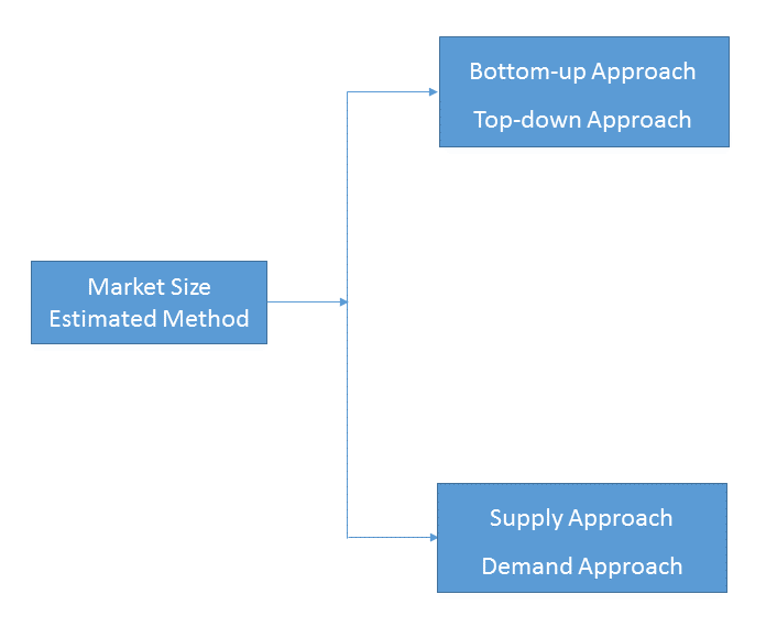
Bottom-up & top-down approach, supply & demand approach are the most important method which is used by HDIN Research to estimate the market size.
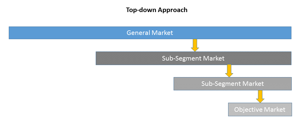
1)Top-down & Bottom-up Approach
Top-down approach uses a general market size figure and determines the percentage that the objective market represents.
Bottom-up approach size the objective market by collecting the sub-segment information.

2)Supply & Demand Approach
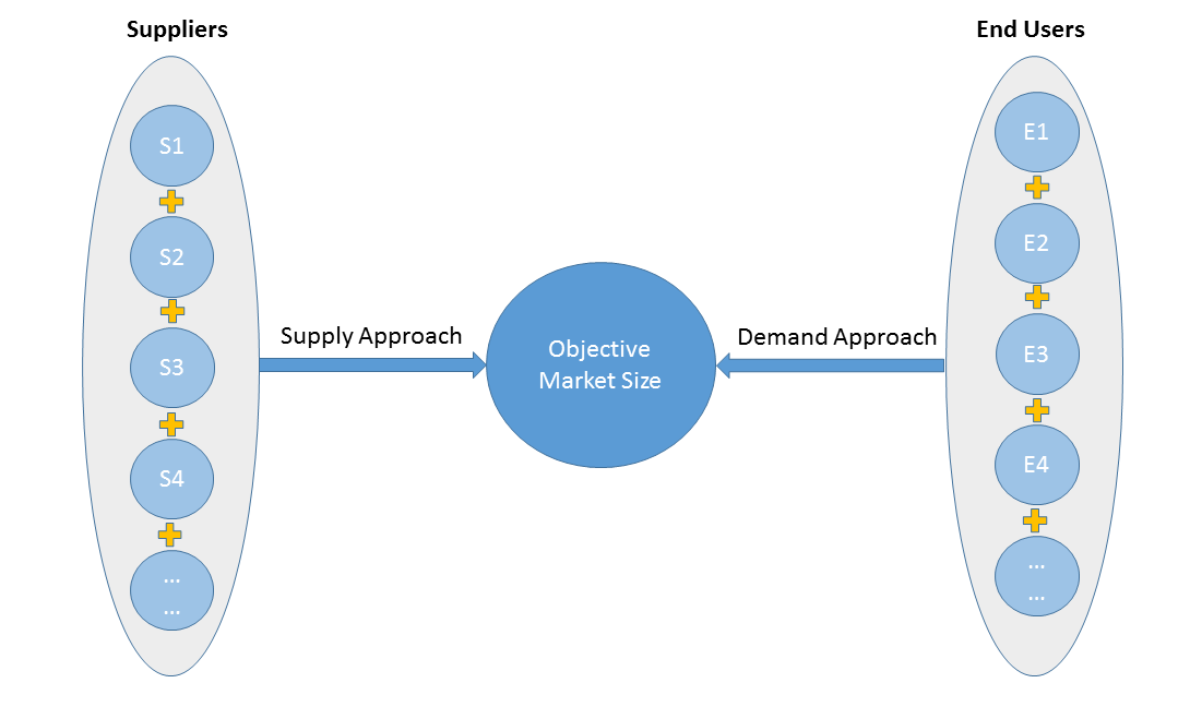
Supply approach is based on assessments of the size of each competitor supplying the objective market.
Demand approach combine end-user data within a market to estimate the objective market size. It is sometimes referred to as bottom-up approach.
- Forecasting Methodology
- Numerous factors impacting the market trend are considered for forecast model:
- New technology and application in the future;
- New project planned/under contraction;
- Global and regional underlying economic growth;
- Threatens of substitute products;
- Industry expert opinion;
- Policy and Society implication.
- Analysis Tools
1)PEST Analysis
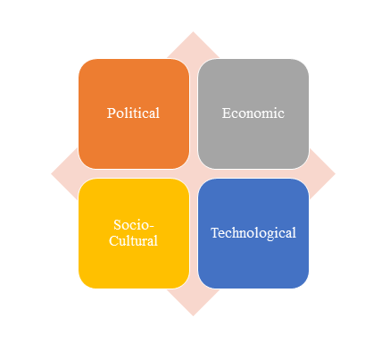
PEST Analysis is a simple and widely used tool that helps our client analyze the Political, Economic, Socio-Cultural, and Technological changes in their business environment.
- Benefits of a PEST analysis:
- It helps you to spot business opportunities, and it gives you advanced warning of significant threats.
- It reveals the direction of change within your business environment. This helps you shape what you’re doing, so that you work with change, rather than against it.
- It helps you avoid starting projects that are likely to fail, for reasons beyond your control.
- It can help you break free of unconscious assumptions when you enter a new country, region, or market; because it helps you develop an objective view of this new environment.
2)Porter’s Five Force Model Analysis
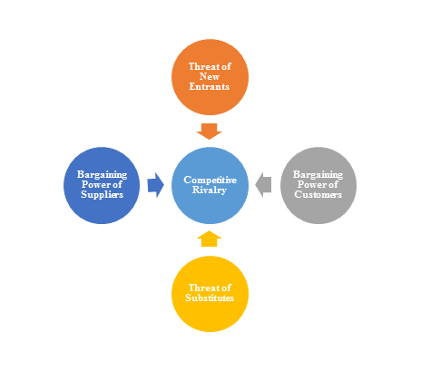
The Porter’s Five Force Model is a tool that can be used to analyze the opportunities and overall competitive advantage. The five forces that can assist in determining the competitive intensity and potential attractiveness within a specific area.
- Threat of New Entrants: Profitable industries that yield high returns will attract new firms.
- Threat of Substitutes: A substitute product uses a different technology to try to solve the same economic need.
- Bargaining Power of Customers: the ability of customers to put the firm under pressure, which also affects the customer's sensitivity to price changes.
- Bargaining Power of Suppliers: Suppliers of raw materials, components, labor, and services (such as expertise) to the firm can be a source of power over the firm when there are few substitutes.
- Competitive Rivalry: For most industries the intensity of competitive rivalry is the major determinant of the competitiveness of the industry.
3)Value Chain Analysis
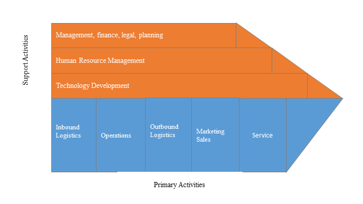
Value chain analysis is a tool to identify activities, within and around the firm and relating these activities to an assessment of competitive strength. Value chain can be analyzed by primary activities and supportive activities. Primary activities include: inbound logistics, operations, outbound logistics, marketing & sales, service. Support activities include: technology development, human resource management, management, finance, legal, planning.
4)SWOT Analysis
SWOT analysis is a tool used to evaluate a company's competitive position by identifying its strengths, weaknesses, opportunities and threats. The strengths and weakness is the inner factor; the opportunities and threats are the external factor. By analyzing the inner and external factors, the analysis can provide the detail information of the position of a player and the characteristics of the industry.
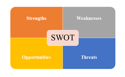
- Strengths describe what the player excels at and separates it from the competition
- Weaknesses stop the player from performing at its optimum level.
- Opportunities refer to favorable external factors that the player can use to give it a competitive advantage.
- Threats refer to factors that have the potential to harm the player.
- Data Sources
| Primary Sources | Secondary Sources |
|---|---|
| Face to face/Phone Interviews with market participants, such as: Manufactures; Distributors; End-users; Experts. Online Survey |
Government/International Organization Data: Annual Report/Presentation/Fact Book Internet Source Information Industry Association Data Free/Purchased Database Market Research Report Book/Journal/News |