Backside Metallization Service Market Insights 2026, Analysis and Forecast to 2031
- Single User License (1 Users) $ 3,500
- Team License (2~5 Users) $ 4,500
- Corporate License (>5 Users) $ 5,500
The semiconductor industry is currently navigating a distinct era of transformation, characterized by the aggressive pursuit of power efficiency, miniaturization, and high-frequency performance. Within this broader ecosystem, the Backside Metallization or BSM service market has emerged as a critical value-added segment. Backside metallization involves the deposition of metallic layers onto the back surface of a semiconductor wafer, typically after it has undergone a thinning process. This process is not merely a structural necessity but a functional imperative for vertical power devices, such as Insulated Gate Bipolar Transistors or IGBTs, Silicon Carbide or SiC MOSFETs, and Gallium Nitride or GaN High-Electron-Mobility Transistors. It creates the necessary electrical contact for the drain or collector, facilitates thermal dissipation, and enables reliable die attachment during the packaging phase.
The market features a high degree of technical specialization. Unlike front-side metallization which defines the intricate circuitry of the logic or memory device, backside metallization focuses on bulk properties: low ohmic contact resistance, high thermal conductivity, and robust adhesion to the thinned substrate. The industry is witnessing a bifurcation in service delivery. One segment caters to the massive volume requirements of silicon-based consumer electronics, where cost-efficiency and throughput are paramount. The other segment addresses the burgeoning demand for wide-bandgap semiconductors in automotive and industrial applications, where the deposition of complex metal stacks—such as Titanium-Nickel-Silver or Gold-Tin alloys—requires advanced physical vapor deposition (PVD) capabilities and stringent quality control.
Based on an in-depth analysis of the supply chain dynamics, capacity utilization rates of major OSATs, and the adoption curves of power electronics in electric vehicles, the global market size for Backside Metallization Services in 2026 is estimated to be between 1.7 billion USD and 3.0 billion USD. The market is projected to expand at a compound annual growth rate or CAGR ranging from 6.8 percent to 9.5 percent over the subsequent forecast period. This growth trajectory is underpinned by the global transition toward electrification, the proliferation of 5G infrastructure requiring efficient RF power amplifiers, and the increasing complexity of heterogeneous packaging which necessitates advanced backside processing.
Recent Industry Developments and Strategic Realignment
The year 2025 has been pivotal for the backend processing landscape, marked by strategic acquisitions and partnerships that underscore the increasing value of specialized wafer services. These developments highlight a trend toward vertical integration and the securing of supply chains for high-reliability and high-performance applications.
On January 15, 2025, Micross Components, Inc., a leading provider of high-reliability microelectronic product and service solutions, completed the acquisition of Integra Technologies. Integra, headquartered in Wichita, Kansas, is an Outsourced Semiconductor Assembly and Test or OSAT provider focused on high-reliability applications. This acquisition is significant for the backside metallization market as it consolidates expertise within the United States domestic supply chain. High-reliability sectors, such as aerospace and defense, require specialized backside metallization schemes, often involving gold or exotic alloys, to ensure device longevity under extreme thermal and mechanical stress. The integration of Integra capabilities allows Micross to offer a comprehensive "one-stop-shop" solution, encompassing thinning, metallization, and final packaging, thereby securing the supply chain for mission-critical components against geopolitical disruptions.
Following this, on August 12, 2025, a technological partnership was announced between Xanadu, a leader in photonic quantum computing, and DISCO Corporation, the renowned manufacturer of precision processing tools. While DISCO is traditionally known for dicing and grinding, this collaboration focuses on developing advanced wafer processing techniques for ultra-low loss photonic integrated chips. The partnership aims to enhance specialized wafer preparation and achieve ultra-smooth surfaces through polishing optimization. In the context of photonics, the backside interface is critical. Although the primary news focuses on surface quality, the implication for metallization is profound. Smooth surfaces are a prerequisite for high-quality backside metal deposition, which is often required for thermal management and electrical grounding in complex photonic circuits. This collaboration signals the market move toward extreme precision, where the interface between the semiconductor and the metal layer must be defect-free to preserve quantum states or optical performance.
Most recently, on August 13, 2025, the ASE Group, the world largest OSAT, acquired a facility from the GaAs foundry WIN Semiconductors in the Southern Taiwan Science Park. Valued at NT 6.5 billion, this acquisition is a strategic expansion to meet the skyrocketing demand for advanced packaging. This move is particularly relevant to the BSM market. WIN Semiconductors specializes in Gallium Arsenide or GaAs, a material critical for RF communications. GaAs devices almost universally require backside gold metallization for grounding and thermal dissipation. By acquiring this facility, ASE not only expands its footprint but potentially inherits or repurposes infrastructure capable of handling compound semiconductors. This positions ASE to aggressively capture the growing demand for RF front-end module packaging and power amplifier assembly, both of which are heavy consumers of backside metallization services.
Value Chain and Industry Ecosystem Analysis
The value chain of the backside metallization market is positioned between wafer fabrication and final assembly, acting as a bridge that transforms a processed wafer into a package-ready component.
The upstream segment involves the suppliers of high-purity sputtering targets and evaporation materials. Metals such as Gold, Silver, Aluminum, Titanium, Nickel, and Vanadium are the primary inputs. The cost structure of the service market is heavily influenced by the fluctuating prices of these precious metals. Additionally, equipment manufacturers play a crucial role, providing the PVD (Sputtering) and Evaporation tools capable of handling thin wafers without breakage.
The midstream segment comprises the service providers. This group is heterogeneous. It includes pure-play foundries that offer BSM as an optional finishing step, large OSATs that integrate BSM into their packaging workflows, and specialized service bureaus that focus exclusively on wafer engineering services (thinning and metallization). Companies like PacTech and specialized divisions within Huahong Group operate here, offering proprietary metal stack recipes optimized for specific bonding requirements.
The downstream segment consists of the device manufacturers and end-users. This includes IDMs (Integrated Device Manufacturers) in the power electronics sector (producing IGBTs and MOSFETs) and fabless design houses developing RF chips and sensors. The requirements from the downstream drive the innovation in the midstream; for instance, the shift from soldering to silver sintering in EV inverters is forcing service providers to develop compatible noble metal backside finishes.
Process Types and Technology Trends
The market is segmented by the deposition technologies employed, each offering distinct advantages depending on the target application and wafer substrate.
● Sputtering Process dominates the market in terms of volume and value. It is the preferred method for depositing complex multi-layer metal stacks (e.g., Ti/NiV/Ag) on silicon and silicon carbide wafers. Sputtering offers superior adhesion and step coverage compared to evaporation. The trend in sputtering is the development of low-temperature processes to prevent damage to the active front-side circuitry and to manage the stress on ultra-thin wafers. High-power impulse magnetron sputtering or HiPIMS is gaining traction for creating denser, defect-free films that improve the barrier properties against solder leaching.
● Evaporation Process remains a critical technology, particularly for the lift-off processes used in compound semiconductors like GaAs and InP, and for depositing thick gold layers. While generally slower and having lower step coverage than sputtering, evaporation is gentler on the wafer surface and is preferred for specific ohmic contact formations in RF devices. The trend here is niche but stable, driven by the communication infrastructure market.
● Others includes electroless plating and electrolytic plating. Plating is often used when a very thick metal layer is required, such as for heat sinks or heavy current-carrying capability. Electroless Nickel Immersion Gold or ENIG is a common plating technique used as a lower-cost alternative to sputtered gold for certain contact applications. This segment is growing in cost-sensitive consumer applications.
Application Analysis and Market Segmentation
The utilization of backside metallization is pervasive across multiple high-growth sectors, each dictating specific material stacks and quality standards.
● Automotive Electronics is currently the most dynamic driver of the BSM market. The electrification of the powertrain relies heavily on power modules. Vertical power devices like IGBTs and SiC MOSFETs conduct current from the front to the back of the chip. Consequently, the quality of the backside metal contact directly determines the device on-resistance and efficiency. The industry is moving toward "solderable front, sinterable back" configurations, requiring service providers to deposit noble metal stacks (like Ag or Au) that facilitate silver sintering, a die attach method capable of withstanding the high operating temperatures of electric vehicles.
● Communication applications, specifically 5G and future 6G networks, generate significant demand. RF Power Amplifiers built on GaAs or GaN-on-SiC substrates require backside metallization for grounding and heat extraction. As base stations become more compact and powerful, the thermal conductivity of the backside metal interface becomes a critical bottleneck, driving demand for high-performance metallization services.
● Industrial applications involve high-voltage drives, traction, and renewable energy inverters. These applications utilize high-power thyristors and IGBTs. The trend is toward larger wafer diameters (transitioning from 200mm to 300mm for standard power devices), which presents a challenge for uniform deposition. Service providers are upgrading their chambers to handle these larger formats while maintaining thickness uniformity.
● Consumer Electronics utilizes BSM primarily for battery protection circuits (MOSFETs) and increasingly for thermal management in compact mobile devices. While the unit cost pressure is high, the sheer volume of smartphones and wearables creates a substantial baseload for the market.
● Others encompasses medical devices and sensors. In medical imaging and sensing, backside metallization is often used for optical blocking or as a distinct electrode in MEMS (Micro-Electro-Mechanical Systems) structures. The focus here is on biocompatibility and precision patterning.
Regional Market Distribution and Geographic Trends
The geographical landscape of the Backside Metallization Service market is heavily concentrated in Asia, mirroring the global semiconductor manufacturing footprint, though strategic pockets exist in the West.
● Asia Pacific is the undisputed leader in market share. Taiwan, China, stands as the epicenter of this activity, driven by the massive capacity of foundries like Vanguard International Semiconductor (VIS) and OSATs like ASE and Chipbond. The ecosystem in Taiwan, China, is highly integrated, allowing for seamless transfer of wafers from fabrication to thinning and metallization. The trend in this region is capacity expansion and the adoption of advanced BSM processes for 300mm wafers to support the AI and HPC boom. The Chinese mainland is also a significant player, with companies like Huahong Group and MACMIC integrating metallization into their power semiconductor workflows. The domestic push for self-sufficiency in power electronics (IGBT and SiC) is fueling rapid growth in BSM capacity within the Chinese mainland.
● North America holds a strategic share focused on high-value, low-volume production. The region is characterized by independent service providers and captive lines serving the aerospace, defense, and medical sectors. Companies like Micross and specialized labs cater to this demand. The trend in North America is the "on-shoring" of advanced packaging services to ensure supply chain security, driven by government incentives and defense requirements.
● Europe maintains a robust position in the automotive power semiconductor market. With major IDMs located in Germany and neighboring countries, there is a strong ecosystem for power device processing. Service providers in Europe, such as PacTech (headquartered in Germany), specialize in advanced packaging technologies including electroless plating and sputtering, specifically tailored for the stringent reliability standards of the European automotive industry.
Key Market Players and Competitive Landscape
The competitive landscape is diverse, featuring a mix of large integrated foundries, comprehensive OSATs, and niche service bureaus.
● Power Master Semiconductor Co. Ltd. serves the power electronics market, focusing on high-efficiency power discrete devices. Their metallization capabilities are likely optimized for high-voltage and high-current applications, supporting their core product lines.
● Enzan Factory Co. Ltd. offers precision wafer processing services. Located in Japan, they leverage the country strong materials science background to provide high-quality thinning and metallization services, likely serving the domestic industrial and sensor markets.
● PacTech (Packaging Technologies GmbH) is a technology leader in wafer-level packaging. Known for their electroless plating and sputtering equipment and services, they provide specialized metallization solutions for flip-chip and power applications. Their ability to offer both equipment and foundry services gives them a unique technical edge.
● Vanguard International Semiconductor Corporation (VIS) is a leading specialty IC foundry in Taiwan, China. They offer backside metallization as part of their turnkey manufacturing services, particularly for their display driver and power management platforms. Their scale allows for high cost-efficiency.
● Axetris serves the micro-optics and MEMS markets. Their metallization services are highly specialized, catering to the precise needs of micro-lens arrays and gas sensors, where standard semiconductor processes might be too aggressive.
● OnChip offers a variety of wafer services including backside processing. They cater to the US market, providing quick-turn services for prototyping and low-volume production, essential for R&D and defense clients.
● Central Semiconductor is a manufacturer of discrete semiconductors. Their involvement implies an internal capability or a specialized service offering for discrete device finishing, ensuring the reliability of their broad product portfolio.
● Prosperity Power Technology Inc. focuses on the heavy-duty power sector. Their metallization processes are tuned for robust adhesion and thick metal layers required for high-power modules used in industrial traction.
● Integrated Service Technology Inc. (iST) is a prominent lab and verification service provider in Taiwan, China. While primarily known for failure analysis, their expansion into backend engineering services allows them to offer specific process steps to troubleshoot or validate new designs.
● CHIPBOND Technology Corporation is a major OSAT in Taiwan, China, specializing in display driver ICs. Backside metallization is a critical step in their gold bumping and COG (Chip-on-Glass) packaging flows, where backside contact is needed for grounding or heat spreading.
● LINCO TECHNOLOGY Co. Ltd. provides sputtering and evaporation services. They are a pure-play service provider in the region, offering flexibility to fabless companies that do not have their own backend infrastructure.
● Huahong Group is a giant in the Chinese semiconductor industry. As a foundry, they offer comprehensive BSM services integrated into their power discrete and analog manufacturing lines, providing a massive capacity base for the domestic market.
● MACMIC (Jiangsu Macmic Electronics) specializes in power electronics. Their metallization capabilities are integral to their IGBT and FRED chip manufacturing, ensuring vertical integration for their power module products.
● Winstek offers a wide range of backend services. As an OSAT, they provide BSM as part of a modular service offering, allowing customers to pick and choose specific process steps to complement their own supply chains.
Downstream Processing and Application Integration
The effectiveness of backside metallization is realized in the subsequent downstream processing steps.
● Wafer Handling and Warpage Control is the immediate challenge following metallization. The deposition of metal layers on a thinned wafer (often <100 microns) introduces stress. If the metal has high tensile or compressive stress, it can cause the wafer to bow significantly, making it impossible for automated handling systems to pick it up for dicing. Service providers must employ stress-engineering techniques, such as adjusting sputtering pressure or depositing counter-stress layers, to keep the wafer flat.
● Ohmic Contact Formation often requires a thermal annealing step after metal deposition. The wafer is heated (sometimes by laser) to form a silicide at the silicon-metal interface, ensuring low electrical resistance. This process must be carefully controlled to avoid melting the metal stack or damaging the front-side devices.
● Die Attach Compatibility is the ultimate test. The top layer of the backside metal stack must be compatible with the die attach material used by the customer. For gold-tin eutectic bonding, a gold surface is required. For silver sintering, a silver or noble-metal surface is needed. For standard solder, a nickel-barrier and silver-finish is common. Service providers must offer a "menu" of metal stacks to match these diverse assembly requirements.
Market Opportunities and Challenges
The Backside Metallization Service market is poised for robust growth but faces complex technical and geopolitical headwinds.
Opportunities are abundant in the realm of Wide Bandgap Semiconductors. The shift from Silicon to Silicon Carbide (SiC) in EVs is a primary growth engine. SiC requires specific metallization recipes (often involving high-temperature annealing) to form good ohmic contacts. Service providers that master the nuances of SiC BSM—specifically achieving low contact resistance on such a hard, wide-bandgap material—will command premium pricing. Additionally, the Medical and Bio-electronics sector offers a high-value niche for biocompatible metallization (like Platinum or Titanium) for implantable devices.
However, the market faces distinct Challenges.
● Trump Tariffs and Trade Policy Impacts represent a significant external threat. The semiconductor supply chain is heavily globalized. The imposition of aggressive tariffs (e.g., 10-20 percent baseline, up to 60 percent on China) under a protectionist US administration would disrupt the cost structure of the BSM market.
* Equipment Costs: Major PVD and evaporation equipment manufacturers are located in Europe and Asia. Tariffs on capital equipment imports to the US would raise the barrier to entry and expansion for domestic service providers like Micross, potentially slowing down the "on-shoring" efforts.
* Consumables: High-purity sputtering targets are often sourced globally. Tariffs on raw materials could squeeze the margins of service providers.
* Supply Chain Bifurcation: High tariffs on wafers processed in China could force US fabless companies to abruptly shift their backend processing to non-China locations (like Taiwan, China, or Southeast Asia), causing capacity bottlenecks and price spikes in those regions. This uncertainty makes long-term capacity planning difficult for service providers.
● Technical Challenges focus on "Thin Wafer Handling." As wafers get thinner (approaching 40 microns for some power devices) and diameters get larger (300mm), the mechanical fragility becomes a dominant issue during the vacuum processing steps of metallization. The risk of wafer breakage inside a sputtering chamber is a high-cost failure mode that service providers must mitigate through advanced clamping and electrostatic chuck technologies.
In summary, the Backside Metallization Service market is a vital, high-tech enabler of the modern electronics industry. It translates the potential of raw semiconductor materials into functional, connectable, and reliable devices. While the industry must navigate the turbulent waters of geopolitical trade wars and the physical limits of handling ultra-thin substrates, the fundamental demand driven by the green energy transition and the connected world ensures a resilient and expanding market trajectory.
Chapter 1 Executive Summary
Chapter 2 Abbreviation and Acronyms
Chapter 3 Preface
3.1 Research Scope
3.2 Research Sources
3.2.1 Data Sources
3.2.2 Assumptions
3.3 Research Method
Chapter 4 Market Landscape
4.1 Market Overview
4.2 Classification/Types
4.3 Application/End Users
Chapter 5 Market Trend Analysis
5.1 introduction
5.2 Drivers
5.3 Restraints
5.4 Opportunities
5.5 Threats
Chapter 6 Industry Chain Analysis
6.1 Upstream/Suppliers Analysis
6.2 Backside Metallization Service Analysis
6.2.1 Technology Analysis
6.2.2 Cost Analysis
6.2.3 Market Channel Analysis
6.3 Downstream Buyers/End Users
Chapter 7 Latest Market Dynamics
7.1 Latest News
7.2 Merger and Acquisition
7.3 Planned/Future Project
7.4 Policy Dynamics
Chapter 8 Historical and Forecast Backside Metallization Service Market in North America (2021-2031)
8.1 Backside Metallization Service Market Size
8.2 Backside Metallization Service Market by End Use
8.3 Competition by Players/Suppliers
8.4 Backside Metallization Service Market Size by Type
8.5 Key Countries Analysis
8.5.1 United States
8.5.2 Canada
8.5.3 Mexico
Chapter 9 Historical and Forecast Backside Metallization Service Market in South America (2021-2031)
9.1 Backside Metallization Service Market Size
9.2 Backside Metallization Service Market by End Use
9.3 Competition by Players/Suppliers
9.4 Backside Metallization Service Market Size by Type
9.5 Key Countries Analysis
9.5.1 Brazil
9.5.2 Argentina
9.5.3 Chile
9.5.4 Peru
Chapter 10 Historical and Forecast Backside Metallization Service Market in Asia & Pacific (2021-2031)
10.1 Backside Metallization Service Market Size
10.2 Backside Metallization Service Market by End Use
10.3 Competition by Players/Suppliers
10.4 Backside Metallization Service Market Size by Type
10.5 Key Countries Analysis
10.5.1 China
10.5.2 India
10.5.3 Japan
10.5.4 South Korea
10.5.5 Southest Asia
10.5.6 Australia
Chapter 11 Historical and Forecast Backside Metallization Service Market in Europe (2021-2031)
11.1 Backside Metallization Service Market Size
11.2 Backside Metallization Service Market by End Use
11.3 Competition by Players/Suppliers
11.4 Backside Metallization Service Market Size by Type
11.5 Key Countries Analysis
11.5.1 Germany
11.5.2 France
11.5.3 United Kingdom
11.5.4 Italy
11.5.5 Spain
11.5.6 Belgium
11.5.7 Netherlands
11.5.8 Austria
11.5.9 Poland
11.5.10 Russia
Chapter 12 Historical and Forecast Backside Metallization Service Market in MEA (2021-2031)
12.1 Backside Metallization Service Market Size
12.2 Backside Metallization Service Market by End Use
12.3 Competition by Players/Suppliers
12.4 Backside Metallization Service Market Size by Type
12.5 Key Countries Analysis
12.5.1 Egypt
12.5.2 Israel
12.5.3 South Africa
12.5.4 Gulf Cooperation Council Countries
12.5.5 Turkey
Chapter 13 Summary For Global Backside Metallization Service Market (2021-2026)
13.1 Backside Metallization Service Market Size
13.2 Backside Metallization Service Market by End Use
13.3 Competition by Players/Suppliers
13.4 Backside Metallization Service Market Size by Type
Chapter 14 Global Backside Metallization Service Market Forecast (2026-2031)
14.1 Backside Metallization Service Market Size Forecast
14.2 Backside Metallization Service Application Forecast
14.3 Competition by Players/Suppliers
14.4 Backside Metallization Service Type Forecast
Chapter 15 Analysis of Global Key Vendors
15.1 Power Master Semiconductor Co. Ltd.
15.1.1 Company Profile
15.1.2 Main Business and Backside Metallization Service Information
15.1.3 SWOT Analysis of Power Master Semiconductor Co. Ltd.
15.1.4 Power Master Semiconductor Co. Ltd. Backside Metallization Service Sales, Revenue, Price and Gross Margin (2021-2026)
15.2 Enzan Factory Co. Ltd.
15.2.1 Company Profile
15.2.2 Main Business and Backside Metallization Service Information
15.2.3 SWOT Analysis of Enzan Factory Co. Ltd.
15.2.4 Enzan Factory Co. Ltd. Backside Metallization Service Sales, Revenue, Price and Gross Margin (2021-2026)
15.3 PacTech
15.3.1 Company Profile
15.3.2 Main Business and Backside Metallization Service Information
15.3.3 SWOT Analysis of PacTech
15.3.4 PacTech Backside Metallization Service Sales, Revenue, Price and Gross Margin (2021-2026)
15.4 Vanguard International Semiconductor Corporation
15.4.1 Company Profile
15.4.2 Main Business and Backside Metallization Service Information
15.4.3 SWOT Analysis of Vanguard International Semiconductor Corporation
15.4.4 Vanguard International Semiconductor Corporation Backside Metallization Service Sales, Revenue, Price and Gross Margin (2021-2026)
15.5 Axetris
15.5.1 Company Profile
15.5.2 Main Business and Backside Metallization Service Information
15.5.3 SWOT Analysis of Axetris
15.5.4 Axetris Backside Metallization Service Sales, Revenue, Price and Gross Margin (2021-2026)
15.6 OnChip
15.6.1 Company Profile
15.6.2 Main Business and Backside Metallization Service Information
15.6.3 SWOT Analysis of OnChip
15.6.4 OnChip Backside Metallization Service Sales, Revenue, Price and Gross Margin (2021-2026)
15.7 Central Semiconductor
15.7.1 Company Profile
15.7.2 Main Business and Backside Metallization Service Information
15.7.3 SWOT Analysis of Central Semiconductor
15.7.4 Central Semiconductor Backside Metallization Service Sales, Revenue, Price and Gross Margin (2021-2026)
15.8 Prosperity Power Technology Inc.
15.8.1 Company Profile
15.8.2 Main Business and Backside Metallization Service Information
15.8.3 SWOT Analysis of Prosperity Power Technology Inc.
15.8.4 Prosperity Power Technology Inc. Backside Metallization Service Sales, Revenue, Price and Gross Margin (2021-2026)
15.9 Integrated Service Technology Inc.
15.9.1 Company Profile
15.9.2 Main Business and Backside Metallization Service Information
15.9.3 SWOT Analysis of Integrated Service Technology Inc.
15.9.4 Integrated Service Technology Inc. Backside Metallization Service Sales, Revenue, Price and Gross Margin (2021-2026)
Please ask for sample pages for full companies list
Table Research Scope of Backside Metallization Service Report
Table Data Sources of Backside Metallization Service Report
Table Major Assumptions of Backside Metallization Service Report
Table Backside Metallization Service Classification
Table Backside Metallization Service Applications
Table Drivers of Backside Metallization Service Market
Table Restraints of Backside Metallization Service Market
Table Opportunities of Backside Metallization Service Market
Table Threats of Backside Metallization Service Market
Table Raw Materials Suppliers
Table Different Production Methods of Backside Metallization Service
Table Cost Structure Analysis of Backside Metallization Service
Table Key End Users
Table Latest News of Backside Metallization Service Market
Table Merger and Acquisition
Table Planned/Future Project of Backside Metallization Service Market
Table Policy of Backside Metallization Service Market
Table 2021-2031 North America Backside Metallization Service Market Size
Table 2021-2031 North America Backside Metallization Service Market Size by Application
Table 2021-2026 North America Backside Metallization Service Key Players Revenue
Table 2021-2026 North America Backside Metallization Service Key Players Market Share
Table 2021-2031 North America Backside Metallization Service Market Size by Type
Table 2021-2031 United States Backside Metallization Service Market Size
Table 2021-2031 Canada Backside Metallization Service Market Size
Table 2021-2031 Mexico Backside Metallization Service Market Size
Table 2021-2031 South America Backside Metallization Service Market Size
Table 2021-2031 South America Backside Metallization Service Market Size by Application
Table 2021-2026 South America Backside Metallization Service Key Players Revenue
Table 2021-2026 South America Backside Metallization Service Key Players Market Share
Table 2021-2031 South America Backside Metallization Service Market Size by Type
Table 2021-2031 Brazil Backside Metallization Service Market Size
Table 2021-2031 Argentina Backside Metallization Service Market Size
Table 2021-2031 Chile Backside Metallization Service Market Size
Table 2021-2031 Peru Backside Metallization Service Market Size
Table 2021-2031 Asia & Pacific Backside Metallization Service Market Size
Table 2021-2031 Asia & Pacific Backside Metallization Service Market Size by Application
Table 2021-2026 Asia & Pacific Backside Metallization Service Key Players Revenue
Table 2021-2026 Asia & Pacific Backside Metallization Service Key Players Market Share
Table 2021-2031 Asia & Pacific Backside Metallization Service Market Size by Type
Table 2021-2031 China Backside Metallization Service Market Size
Table 2021-2031 India Backside Metallization Service Market Size
Table 2021-2031 Japan Backside Metallization Service Market Size
Table 2021-2031 South Korea Backside Metallization Service Market Size
Table 2021-2031 Southeast Asia Backside Metallization Service Market Size
Table 2021-2031 Australia Backside Metallization Service Market Size
Table 2021-2031 Europe Backside Metallization Service Market Size
Table 2021-2031 Europe Backside Metallization Service Market Size by Application
Table 2021-2026 Europe Backside Metallization Service Key Players Revenue
Table 2021-2026 Europe Backside Metallization Service Key Players Market Share
Table 2021-2031 Europe Backside Metallization Service Market Size by Type
Table 2021-2031 Germany Backside Metallization Service Market Size
Table 2021-2031 France Backside Metallization Service Market Size
Table 2021-2031 United Kingdom Backside Metallization Service Market Size
Table 2021-2031 Italy Backside Metallization Service Market Size
Table 2021-2031 Spain Backside Metallization Service Market Size
Table 2021-2031 Belgium Backside Metallization Service Market Size
Table 2021-2031 Netherlands Backside Metallization Service Market Size
Table 2021-2031 Austria Backside Metallization Service Market Size
Table 2021-2031 Poland Backside Metallization Service Market Size
Table 2021-2031 Russia Backside Metallization Service Market Size
Table 2021-2031 MEA Backside Metallization Service Market Size
Table 2021-2031 MEA Backside Metallization Service Market Size by Application
Table 2021-2026 MEA Backside Metallization Service Key Players Revenue
Table 2021-2026 MEA Backside Metallization Service Key Players Market Share
Table 2021-2031 MEA Backside Metallization Service Market Size by Type
Table 2021-2031 Egypt Backside Metallization Service Market Size
Table 2021-2031 Israel Backside Metallization Service Market Size
Table 2021-2031 South Africa Backside Metallization Service Market Size
Table 2021-2031 Gulf Cooperation Council Countries Backside Metallization Service Market Size
Table 2021-2031 Turkey Backside Metallization Service Market Size
Table 2021-2026 Global Backside Metallization Service Market Size by Region
Table 2021-2026 Global Backside Metallization Service Market Size Share by Region
Table 2021-2026 Global Backside Metallization Service Market Size by Application
Table 2021-2026 Global Backside Metallization Service Market Share by Application
Table 2021-2026 Global Backside Metallization Service Key Vendors Revenue
Table 2021-2026 Global Backside Metallization Service Key Vendors Market Share
Table 2021-2026 Global Backside Metallization Service Market Size by Type
Table 2021-2026 Global Backside Metallization Service Market Share by Type
Table 2026-2031 Global Backside Metallization Service Market Size by Region
Table 2026-2031 Global Backside Metallization Service Market Size Share by Region
Table 2026-2031 Global Backside Metallization Service Market Size by Application
Table 2026-2031 Global Backside Metallization Service Market Share by Application
Table 2026-2031 Global Backside Metallization Service Key Vendors Revenue
Table 2026-2031 Global Backside Metallization Service Key Vendors Market Share
Table 2026-2031 Global Backside Metallization Service Market Size by Type
Table 2026-2031 Backside Metallization Service Global Market Share by Type
Figure Market Size Estimated Method
Figure Major Forecasting Factors
Figure Backside Metallization Service Picture
Figure 2021-2031 North America Backside Metallization Service Market Size and CAGR
Figure 2021-2031 South America Backside Metallization Service Market Size and CAGR
Figure 2021-2031 Asia & Pacific Backside Metallization Service Market Size and CAGR
Figure 2021-2031 Europe Backside Metallization Service Market Size and CAGR
Figure 2021-2031 MEA Backside Metallization Service Market Size and CAGR
Figure 2021-2026 Global Backside Metallization Service Market Size and Growth Rate
Figure 2026-2031 Global Backside Metallization Service Market Size and Growth Rate
Research Methodology
- Market Estimated Methodology:
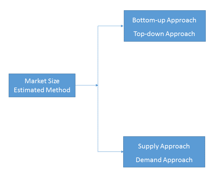
Bottom-up & top-down approach, supply & demand approach are the most important method which is used by HDIN Research to estimate the market size.
1)Top-down & Bottom-up Approach
Top-down approach uses a general market size figure and determines the percentage that the objective market represents.
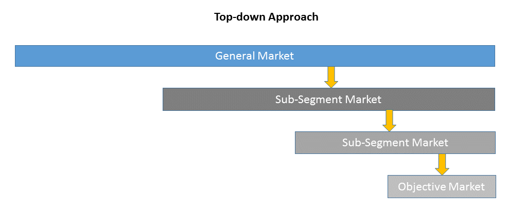
Bottom-up approach size the objective market by collecting the sub-segment information.

2)Supply & Demand Approach
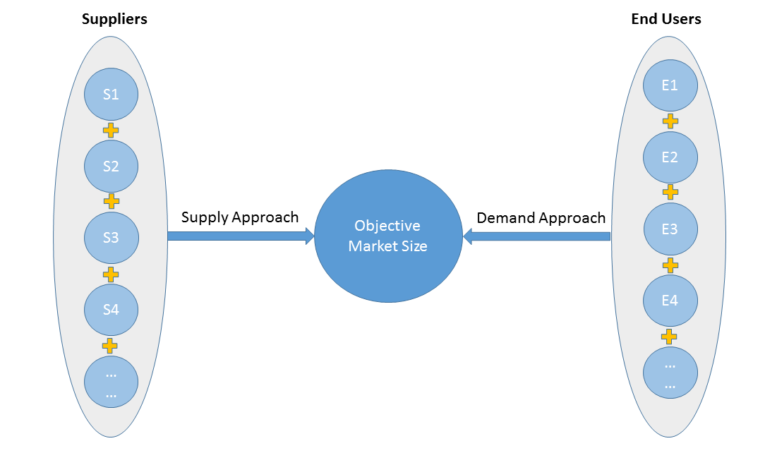
Supply approach is based on assessments of the size of each competitor supplying the objective market.
Demand approach combine end-user data within a market to estimate the objective market size. It is sometimes referred to as bottom-up approach.
- Forecasting Methodology
- Numerous factors impacting the market trend are considered for forecast model:
- New technology and application in the future;
- New project planned/under contraction;
- Global and regional underlying economic growth;
- Threatens of substitute products;
- Industry expert opinion;
- Policy and Society implication.
- Analysis Tools
1)PEST Analysis
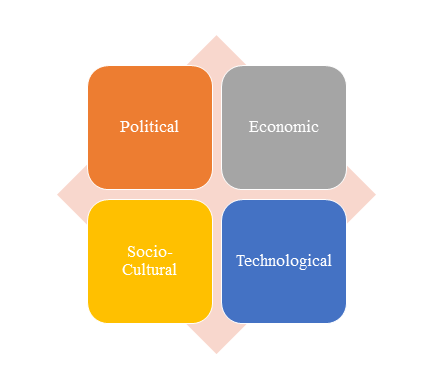
PEST Analysis is a simple and widely used tool that helps our client analyze the Political, Economic, Socio-Cultural, and Technological changes in their business environment.
- Benefits of a PEST analysis:
- It helps you to spot business opportunities, and it gives you advanced warning of significant threats.
- It reveals the direction of change within your business environment. This helps you shape what you’re doing, so that you work with change, rather than against it.
- It helps you avoid starting projects that are likely to fail, for reasons beyond your control.
- It can help you break free of unconscious assumptions when you enter a new country, region, or market; because it helps you develop an objective view of this new environment.
2)Porter’s Five Force Model Analysis
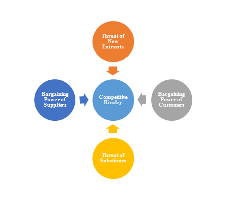
The Porter’s Five Force Model is a tool that can be used to analyze the opportunities and overall competitive advantage. The five forces that can assist in determining the competitive intensity and potential attractiveness within a specific area.
- Threat of New Entrants: Profitable industries that yield high returns will attract new firms.
- Threat of Substitutes: A substitute product uses a different technology to try to solve the same economic need.
- Bargaining Power of Customers: the ability of customers to put the firm under pressure, which also affects the customer's sensitivity to price changes.
- Bargaining Power of Suppliers: Suppliers of raw materials, components, labor, and services (such as expertise) to the firm can be a source of power over the firm when there are few substitutes.
- Competitive Rivalry: For most industries the intensity of competitive rivalry is the major determinant of the competitiveness of the industry.
3)Value Chain Analysis
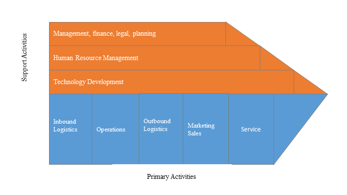
Value chain analysis is a tool to identify activities, within and around the firm and relating these activities to an assessment of competitive strength. Value chain can be analyzed by primary activities and supportive activities. Primary activities include: inbound logistics, operations, outbound logistics, marketing & sales, service. Support activities include: technology development, human resource management, management, finance, legal, planning.
4)SWOT Analysis
SWOT analysis is a tool used to evaluate a company's competitive position by identifying its strengths, weaknesses, opportunities and threats. The strengths and weakness is the inner factor; the opportunities and threats are the external factor. By analyzing the inner and external factors, the analysis can provide the detail information of the position of a player and the characteristics of the industry.
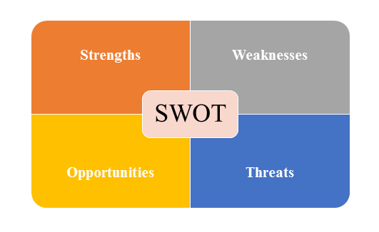
- Strengths describe what the player excels at and separates it from the competition
- Weaknesses stop the player from performing at its optimum level.
- Opportunities refer to favorable external factors that the player can use to give it a competitive advantage.
- Threats refer to factors that have the potential to harm the player.
- Data Sources
| Primary Sources | Secondary Sources |
|---|---|
| Face to face/Phone Interviews with market participants, such as: Manufactures; Distributors; End-users; Experts. Online Survey |
Government/International Organization Data: Annual Report/Presentation/Fact Book Internet Source Information Industry Association Data Free/Purchased Database Market Research Report Book/Journal/News |