Semiconductor Photomask Glass Substrate Market Insights 2026, Analysis and Forecast to 2031
- Single User License (1 Users) $ 3,500
- Team License (2~5 Users) $ 4,500
- Corporate License (>5 Users) $ 5,500
The semiconductor industry serves as the bedrock of the modern digital economy, and sitting at the very foundation of this complex manufacturing chain is the semiconductor photomask glass substrate market. Photomasks are the master plates used to transfer circuit patterns onto semiconductor wafers during the lithography process. The quality, purity, and thermal stability of the glass substrate used to create these photomasks are absolute determinants of the final chip performance. As the industry advances toward smaller nodes, specifically in the realm of extreme ultraviolet or EUV lithography and deep ultraviolet or DUV lithography, the requirements for these glass substrates have transitioned from standard borosilicate glass to ultra-high purity synthetic fused silica and modified quartz materials. These materials must exhibit near-zero thermal expansion, exceptional optical transmission at specific wavelengths, and pristine surface flatness to ensure that nanometer-scale circuit designs are reproduced without distortion.
The market for semiconductor photomask glass substrates is characterized by an oligopolistic supply structure on the upstream side, dominated by a few global glass manufacturers with the chemical and thermal engineering pedigree to produce synthetic quartz. However, the downstream demand is diversifying. While traditional integrated circuit fabrication remains the primary driver, there is a surging demand for photomask glass in advanced packaging applications, Micro-Electro-Mechanical Systems or MEMS, and photonics. Furthermore, the material technology is evolving beyond just lithography masks; the industry is witnessing a paradigm shift where glass is being investigated and adopted as a core substrate material for chip packaging itself, replacing organic cores to facilitate finer line widths and better thermal management.
Based on a comprehensive analysis of the semiconductor material supply chain, the expansion of foundry capacities globally, and the capital expenditure trends of major mask shops, the global market size for Semiconductor Photomask Glass Substrates in the year 2025 is estimated to be in the range of 1.9 billion USD to 3.5 billion USD. This valuation encompasses the raw glass blanks and prepared substrates used for both front-end wafer fabrication masks and back-end packaging masks. The market is projected to grow at a Compound Annual Growth Rate or CAGR estimated between 5.8 percent and 8.4 percent over the subsequent forecast period. This growth is underpinned by the increasing layer count in 3D NAND and logic chips, which necessitates a higher number of masks per wafer start, and the booming domestic semiconductor manufacturing initiatives in regions like the Chinese mainland.
Recent Industry Developments and Strategic Expansion
The landscape of the semiconductor glass market in 2025 has been defined by a dual focus: expanding capacity for traditional lithography needs and pioneering new applications for glass in advanced packaging. The latter trend is reshaping the definition of the market, as glass transitions from being just a tool for transfer (mask) to a structural component of the chip package (substrate).
According to recent industry data, the broader global semiconductor photomask market—the direct downstream consumer of these glass substrates—has reached a scale of approximately 8.94 billion USD. Within this global context, the market in the Chinese mainland has emerged as a powerhouse, valued at approximately 2.3 billion USD, which constitutes a share exceeding 20 percent of the global total. This growth rate in the Chinese mainland is currently leading the world, driven by the aggressive expansion of mature node capacities and the rapid development of domestic supply chains. A granular look at this consumption reveals that the wafer manufacturing segment accounts for the lion share, utilizing approximately 1.5 billion USD worth of masks, while the packaging segment consumes around 0.4 billion USD, and other device applications contribute 0.9 billion USD. This data underscores the critical volume demand for high-quality glass substrates to feed this expanding mask production ecosystem.
Against this backdrop of robust demand, significant technological pivots occurred in late 2025, specifically regarding the use of glass in next-generation packaging. On December 16, 2025, Dai Nippon Printing Co., Ltd. or DNP announced the launch of a new pilot production line for Through Glass Via or TGV glass core substrates. Located at its Kuki Plant in Saitama Prefecture, Japan, this facility is designed to address the needs of next-generation semiconductor packaging, which requires higher interconnect density than organic substrates can provide. The new line is scheduled to commence phased operations starting in December 2025. This strategic move is aimed at enabling mass-production verification and initiating the shipment of high-quality samples by early 2026. This development signifies a major expansion in the total addressable market for semiconductor-grade glass, moving beyond temporary masks to permanent package cores.
Following closely on December 17, 2025, TOPPAN Inc., a subsidiary of TOPPAN Holdings Inc., announced the completion of a new manufacturing line at its Niigata Plant in Shibata, Niigata Prefecture, Japan. This line is dedicated to Flip Chip-Ball Grid Array or FC-BGA substrates, a high-density packaging format essential for high-performance computing and AI processors. While traditional FC-BGA uses organic cores, the industry trajectory suggests a convergence where glass-handling expertise from the photomask sector is being leveraged for these advanced substrates. The new line is set to come online in January 2026, further cementing Japan position as the hub for high-tech substrate manufacturing.
Value Chain and Industry Ecosystem Analysis
The value chain for semiconductor photomask glass substrates is vertically deep and technologically exclusive.
The upstream segment begins with the synthesis of raw materials. Unlike standard glass made from silica sand, semiconductor-grade fused silica is produced from high-purity chemical precursors like silicon tetrachloride or silane. This chemical synthesis allows for the creation of glass with impurity levels measured in parts per billion. This stage is controlled by major chemical and material science conglomerates.
The midstream segment involves the melting, forming, and initial processing of the glass. This is the domain of the key market players who possess proprietary furnace technologies. The glass is formed into large boules or ingots, which are then sliced into rough blanks. The critical value-add here is the control of homogeneity and thermal expansion characteristics. Following the forming, the rough blanks undergo grinding, lapping, and precision polishing. This is a vital step, as the surface roughness must be minimized to Angstrom levels to prevent optical aberrations during lithography. Companies often specialize in either the material formation or the precision polishing, though some integrate both.
The downstream integration involves the "Mask Blanks" manufacturers. These companies take the polished glass substrate and deposit the necessary absorber layers (such as chrome or molybdenum silicide) and photoresist. These blanks are then sold to "Mask Shops"—either captive shops owned by foundries (like those of TSMC or Intel) or merchant shops (like DNP, Toppan, or Photronics). Finally, the written photomask is used in the wafer fab.
A parallel value chain is emerging for Glass Core Substrates, where the glass is not just polished but micro-structured (via TGV technology) to serve as the interposer or core of the chip package, directly linking the glass manufacturers to OSATs (Outsourced Semiconductor Assembly and Test providers).
Application Analysis and Market Segmentation
The utilization of semiconductor glass substrates is segmented by the distinct requirements of the final device being fabricated.
● Masks for MEMS require glass substrates that can withstand deep reactive ion etching and exhibit high chemical resistance. Unlike standard IC masks, MEMS masks often define three-dimensional mechanical structures. Consequently, the glass substrates used here may differ in thickness and optical properties, often requiring borosilicate variants that match the thermal expansion of silicon to prevent warping during high-temperature bonding processes. The trend in this segment is toward larger substrate sizes to accommodate the shift of MEMS manufacturing from 150mm to 200mm and 300mm wafers.
● Masks for Semiconductor Packaging are the fastest-growing application segment. This encompasses masks used for Re-distribution Layer or RDL formation in Fan-Out Wafer-Level Packaging and substrates for glass interposers. As indicated by the market data, while this segment is currently smaller (0.4 billion USD in mask value) compared to wafer fabrication, it is expanding rapidly due to the chiplet revolution. The glass requirements here prioritize dimensional stability over large areas, as panel-level packaging moves to formats larger than traditional silicon wafers.
● Masks for LED and Display applications utilize larger, rectangular glass substrates. While the resolution requirements for LED lithography are generally lower than for advanced logic, the cost pressure is significantly higher. This segment demands high-throughput glass solutions, often utilizing lower-cost quartz or high-grade soda-lime glass for non-critical layers. The trend is toward ultra-large format masks to support the manufacturing of Mini-LED and Micro-LED displays.
● Others includes applications in photonics, optical sensors, and microfluidics. In photonics, the glass substrate is often used to pattern waveguides. This niche demands glass with specific refractive indices and extremely low optical loss.
Regional Market Distribution and Geographic Trends
The geographical distribution of the semiconductor photomask glass substrate market is heavily skewed toward the Asia-Pacific region, mirroring the concentration of global wafer capacity.
● Asia Pacific is the dominant region, accounting for the majority of global consumption. Japan holds a unique position as the primary supplier of the high-purity glass material itself, home to leaders like Asahi Glass, Nippon Electric Glass, and Hoya. The manufacturing excellence and intellectual property regarding synthetic quartz synthesis are deeply rooted in Japan. Taiwan, China, represents the largest consumption hub for high-end photomask substrates, driven by its unparalleled foundry ecosystem. The demand here is for the most advanced EUV-grade glass blanks. The Chinese mainland is the fastest-growing market, as evidenced by the 2.3 billion USD mask market size. The trend in the Chinese mainland is a massive uptake of DUV-grade quartz substrates to support the build-out of 28nm and mature node capacities. South Korea remains a critical market, primarily driven by memory manufacturers requiring high volumes of masks for 3D NAND stacking.
● North America retains a strategic share, focused on R&D and high-value manufacturing. The US is home to key material innovators like Corning. The market trend in North America is influenced by the "Chips Act" and efforts to re-shore semiconductor manufacturing. This is creating renewed demand for domestic mask infrastructure and the requisite glass substrates, particularly for defense and high-reliability applications.
● Europe has a smaller volume share but plays a critical role in the equipment and optics supply chain (e.g., ASML ecosystem). German manufacturers like SCHOTT are pivotal in providing the specialized low-thermal-expansion glass ceramics used in EUV lithography mirrors and mask substrates. The trend in Europe is focused on specialized automotive and industrial sensor applications.
Key Market Players and Competitive Landscape
The competitive landscape is defined by a small number of highly specialized players who have mastered the difficult art of glass science.
● SCHOTT is a global technology group based in Germany, renowned for its optical glass and glass-ceramics. In this market, SCHOTT provides high-homogeneity fused silica and specialized low-expansion materials that are critical for high-precision lithography. Their "ZERODUR" glass-ceramic is an industry benchmark for thermal stability.
● Nippon Electric Glass or NEG is a leading Japanese manufacturer. They produce a wide range of glass products for electronic displays and semiconductor applications. NEG has been aggressive in developing glass substrates that are compatible with the specific chemical and thermal rigors of semiconductor processing.
● Asahi Glass Co or AGC, now operating under the AGC Inc. brand, is a titan in the glass industry. They are one of the few companies capable of mass-producing synthetic fused silica with the purity required for ArF immersion and EUV lithography. AGC integrated production capability, from raw material to polished blank, gives them a significant cost and quality advantage.
● Corning is a premier American materials science company. Their High Purity Fused Silica or HPFS is a standard material in the semiconductor industry, known for its exceptional optical transmission and resistance to laser damage. Corning is also heavily involved in developing glass cores for advanced packaging, leveraging their display glass expertise.
● Tecnisco specializes in processing glass and silicon. They offer precision dicing and structuring services, providing customized glass substrates with micro-features for MEMS and sensor applications.
● Plan Optik AG is a German company focusing on structured wafers. They are a market leader in supplying glass wafers for MEMS encapsulation and microfluidics. Their products are often pre-structured or bonded, offering high value to MEMS foundries.
● Bullen Ultrasonics is known for its ultrasonic machining capabilities. While not a glass maker, they are a critical service provider in the value chain, capable of drilling and machining semiconductor glass for complex components and sensors.
● Swift Glass is a US-based fabricator offering custom glass parts. They serve the lower-volume, high-mix segment of the market, providing specialized substrates for optical and industrial electronic applications.
● Coresix Precision Glass specializes in the precision fabrication of glass components. They provide custom-sized glass wafers and substrates with high surface quality, serving the optical and semiconductor sectors.
● Absolics, a subsidiary of SKC, is a key player to watch in the packaging space. They are pioneering the commercialization of glass core substrates for high-performance computing. Their inclusion underscores the market shift toward glass-based packaging solutions.
● Hoya Corporation is a dominant force in the mask blank market. While they purchase raw glass, their value-add in polishing and coating makes them a critical node. Hoya effectively controls a large portion of the global supply of finished mask blanks, serving both merchant and captive mask shops.
● Sydor Optics specializes in custom flat optics. They provide high-precision windows and substrates, catering to the photonics and research sectors of the semiconductor market.
Downstream Processing and Application Integration
The integration of glass substrates into the downstream workflow involves several critical processing steps that define the final utility of the material.
● Polishing and Flatness Control is the most critical downstream process. The glass substrate must be polished to a flatness often measured in fractions of a micron across the entire surface. Any deviation or "bow" in the glass will result in focus errors during the lithography process. For EUV applications, the flatness requirements are even more stringent to prevent placement errors. Suppliers are investing in Magnetorheological Finishing or MRF technology to achieve these sub-nanometer surface figures.
● Coating and Blank Preparation involves the deposition of the optical stack. For standard photomasks, this involves sputtering a layer of chromium (the absorber) and applying a photoresist. The adhesion of these layers to the glass substrate is paramount. The glass surface chemistry must be modified to ensure zero peeling or pinhole defects.
● Through Glass Via or TGV Formation is the key integration step for the new glass core packaging market. This involves creating microscopic holes in the glass substrate to allow electrical vertical interconnects. Unlike silicon which is conductive, glass is an insulator, making it an excellent dielectric. However, drilling glass without cracking is difficult. Technologies like Laser Induced Deep Etching or LIDE are being integrated to create high-aspect-ratio vias, enabling the DNP and Toppan developments mentioned earlier.
Market Opportunities and Challenges
The Semiconductor Photomask Glass Substrate market is poised for significant opportunities driven by the physical limits of Moore Law. The transition to High-NA EUV lithography creates a demand for new types of mask substrates with even lower thermal expansion coefficients and higher mechanical rigidity. Furthermore, the "Glass Core" revolution in packaging presents a massive greenfield opportunity. If glass substrates replace organic cores in data center CPUs and GPUs, the volume of glass consumption in the semiconductor sector could multiply exponentially.
However, the market faces substantial challenges.
● Technical Challenges focus on the brittleness and handling of glass. Unlike silicon, which has a well-established ecosystem of handling robots and chucks, glass requires specialized handling to prevent edge chipping and breakage. In the context of packaging, the lack of a mature supply chain for large-format glass panels (typically 510mm x 515mm) creates a bottleneck for mass adoption.
● The Impact of Trump Tariffs creates a geopolitical complexity. With a significant portion of high-grade synthetic quartz and finished mask blanks originating from Japan and being processed in China (as indicated by the 2.3 billion USD market size in the Chinese mainland), US tariffs introduce supply chain friction.
* Tariffs on Raw Materials: If the US administration imposes tariffs on imported glass materials from Japan or Europe, US-based mask shops and defense contractors could face rising input costs.
* Tariffs on Finished Goods: The 60 percent tariff threat on goods from the Chinese mainland is particularly disruptive. Many US fabless companies utilize wafer foundries and mask shops in the Chinese mainland for mature nodes. High tariffs would force these companies to relocate their mask sourcing to Taiwan, China, or back to the US/Europe, potentially overwhelming the capacity of non-Chinese suppliers. This bifurcation of the supply chain forces global glass manufacturers to maintain dual inventories and navigate complex export control compliance, increasing the overall cost structure of the industry.
In summary, the Semiconductor Photomask Glass Substrate market is a highly specialized, technology-intensive sector that acts as the gatekeeper for chip manufacturing. While it anchors the traditional lithography process, it is simultaneously branching out to become the backbone of advanced packaging. The interplay between Japanese material mastery, the manufacturing scale of the Chinese mainland and Taiwan, China, and the strategic imperatives of the US creates a dynamic, albeit volatile, market environment.
Chapter 1 Executive Summary
Chapter 2 Abbreviation and Acronyms
Chapter 3 Preface
3.1 Research Scope
3.2 Research Sources
3.2.1 Data Sources
3.2.2 Assumptions
3.3 Research Method
Chapter 4 Market Landscape
4.1 Market Overview
4.2 Classification/Types
4.3 Application/End Users
Chapter 5 Market Trend Analysis
5.1 introduction
5.2 Drivers
5.3 Restraints
5.4 Opportunities
5.5 Threats
Chapter 6 Industry Chain Analysis
6.1 Upstream/Suppliers Analysis
6.2 Semiconductor Photomask Glass Substrate Analysis
6.2.1 Technology Analysis
6.2.2 Cost Analysis
6.2.3 Market Channel Analysis
6.3 Downstream Buyers/End Users
Chapter 7 Latest Market Dynamics
7.1 Latest News
7.2 Merger and Acquisition
7.3 Planned/Future Project
7.4 Policy Dynamics
Chapter 8 Trading Analysis
8.1 Export of Semiconductor Photomask Glass Substrate by Region
8.2 Import of Semiconductor Photomask Glass Substrate by Region
8.3 Balance of Trade
Chapter 9 Historical and Forecast Semiconductor Photomask Glass Substrate Market in North America (2021-2031)
9.1 Semiconductor Photomask Glass Substrate Market Size
9.2 Semiconductor Photomask Glass Substrate Demand by End Use
9.3 Competition by Players/Suppliers
9.4 Type Segmentation and Price
9.5 Key Countries Analysis
9.5.1 United States
9.5.2 Canada
9.5.3 Mexico
Chapter 10 Historical and Forecast Semiconductor Photomask Glass Substrate Market in South America (2021-2031)
10.1 Semiconductor Photomask Glass Substrate Market Size
10.2 Semiconductor Photomask Glass Substrate Demand by End Use
10.3 Competition by Players/Suppliers
10.4 Type Segmentation and Price
10.5 Key Countries Analysis
10.5.1 Brazil
10.5.2 Argentina
10.5.3 Chile
10.5.4 Peru
Chapter 11 Historical and Forecast Semiconductor Photomask Glass Substrate Market in Asia & Pacific (2021-2031)
11.1 Semiconductor Photomask Glass Substrate Market Size
11.2 Semiconductor Photomask Glass Substrate Demand by End Use
11.3 Competition by Players/Suppliers
11.4 Type Segmentation and Price
11.5 Key Countries Analysis
11.5.1 China
11.5.2 India
11.5.3 Japan
11.5.4 South Korea
11.5.5 Southest Asia
11.5.6 Australia
Chapter 12 Historical and Forecast Semiconductor Photomask Glass Substrate Market in Europe (2021-2031)
12.1 Semiconductor Photomask Glass Substrate Market Size
12.2 Semiconductor Photomask Glass Substrate Demand by End Use
12.3 Competition by Players/Suppliers
12.4 Type Segmentation and Price
12.5 Key Countries Analysis
12.5.1 Germany
12.5.2 France
12.5.3 United Kingdom
12.5.4 Italy
12.5.5 Spain
12.5.6 Belgium
12.5.7 Netherlands
12.5.8 Austria
12.5.9 Poland
12.5.10 Russia
Chapter 13 Historical and Forecast Semiconductor Photomask Glass Substrate Market in MEA (2021-2031)
13.1 Semiconductor Photomask Glass Substrate Market Size
13.2 Semiconductor Photomask Glass Substrate Demand by End Use
13.3 Competition by Players/Suppliers
13.4 Type Segmentation and Price
13.5 Key Countries Analysis
13.5.1 Egypt
13.5.2 Israel
13.5.3 South Africa
13.5.4 Gulf Cooperation Council Countries
13.5.5 Turkey
Chapter 14 Summary For Global Semiconductor Photomask Glass Substrate Market (2021-2026)
14.1 Semiconductor Photomask Glass Substrate Market Size
14.2 Semiconductor Photomask Glass Substrate Demand by End Use
14.3 Competition by Players/Suppliers
14.4 Type Segmentation and Price
Chapter 15 Global Semiconductor Photomask Glass Substrate Market Forecast (2026-2031)
15.1 Semiconductor Photomask Glass Substrate Market Size Forecast
15.2 Semiconductor Photomask Glass Substrate Demand Forecast
15.3 Competition by Players/Suppliers
15.4 Type Segmentation and Price Forecast
Chapter 16 Analysis of Global Key Vendors
15.1 SCHOTT
15.1.1 Company Profile
15.1.2 Main Business and Semiconductor Photomask Glass Substrate Information
15.1.3 SWOT Analysis of SCHOTT
15.1.4 SCHOTT Semiconductor Photomask Glass Substrate Sales, Revenue, Price and Gross Margin (2021-2026)
15.2 Nippon Electric Glass
15.2.1 Company Profile
15.2.2 Main Business and Semiconductor Photomask Glass Substrate Information
15.2.3 SWOT Analysis of Nippon Electric Glass
15.2.4 Nippon Electric Glass Semiconductor Photomask Glass Substrate Sales, Revenue, Price and Gross Margin (2021-2026)
15.3 Asahi Glass Co
15.3.1 Company Profile
15.3.2 Main Business and Semiconductor Photomask Glass Substrate Information
15.3.3 SWOT Analysis of Asahi Glass Co
15.3.4 Asahi Glass Co Semiconductor Photomask Glass Substrate Sales, Revenue, Price and Gross Margin (2021-2026)
15.4 Corning
15.4.1 Company Profile
15.4.2 Main Business and Semiconductor Photomask Glass Substrate Information
15.4.3 SWOT Analysis of Corning
15.4.4 Corning Semiconductor Photomask Glass Substrate Sales, Revenue, Price and Gross Margin (2021-2026)
15.5 Tecnisco
15.5.1 Company Profile
15.5.2 Main Business and Semiconductor Photomask Glass Substrate Information
15.5.3 SWOT Analysis of Tecnisco
15.5.4 Tecnisco Semiconductor Photomask Glass Substrate Sales, Revenue, Price and Gross Margin (2021-2026)
15.6 Plan Optik AG
15.6.1 Company Profile
15.6.2 Main Business and Semiconductor Photomask Glass Substrate Information
15.6.3 SWOT Analysis of Plan Optik AG
15.6.4 Plan Optik AG Semiconductor Photomask Glass Substrate Sales, Revenue, Price and Gross Margin (2021-2026)
15.7 Bullen
15.7.1 Company Profile
15.7.2 Main Business and Semiconductor Photomask Glass Substrate Information
15.7.3 SWOT Analysis of Bullen
15.7.4 Bullen Semiconductor Photomask Glass Substrate Sales, Revenue, Price and Gross Margin (2021-2026)
15.8 Swift Glass
15.8.1 Company Profile
15.8.2 Main Business and Semiconductor Photomask Glass Substrate Information
15.8.3 SWOT Analysis of Swift Glass
15.8.4 Swift Glass Semiconductor Photomask Glass Substrate Sales, Revenue, Price and Gross Margin (2021-2026)
Please ask for sample pages for full companies list
Table Research Scope of Semiconductor Photomask Glass Substrate Report
Table Data Sources of Semiconductor Photomask Glass Substrate Report
Table Major Assumptions of Semiconductor Photomask Glass Substrate Report
Table Semiconductor Photomask Glass Substrate Classification
Table Semiconductor Photomask Glass Substrate Applications List
Table Drivers of Semiconductor Photomask Glass Substrate Market
Table Restraints of Semiconductor Photomask Glass Substrate Market
Table Opportunities of Semiconductor Photomask Glass Substrate Market
Table Threats of Semiconductor Photomask Glass Substrate Market
Table Raw Materials Suppliers List
Table Different Production Methods of Semiconductor Photomask Glass Substrate
Table Cost Structure Analysis of Semiconductor Photomask Glass Substrate
Table Key End Users List
Table Latest News of Semiconductor Photomask Glass Substrate Market
Table Merger and Acquisition List
Table Planned/Future Project of Semiconductor Photomask Glass Substrate Market
Table Policy of Semiconductor Photomask Glass Substrate Market
Table 2021-2031 Regional Export of Semiconductor Photomask Glass Substrate
Table 2021-2031 Regional Import of Semiconductor Photomask Glass Substrate
Table 2021-2031 Regional Trade Balance
Table 2021-2031 North America Semiconductor Photomask Glass Substrate Market Size and Market Volume List
Table 2021-2031 North America Semiconductor Photomask Glass Substrate Demand List by Application
Table 2021-2026 North America Semiconductor Photomask Glass Substrate Key Players Sales List
Table 2021-2026 North America Semiconductor Photomask Glass Substrate Key Players Market Share List
Table 2021-2031 North America Semiconductor Photomask Glass Substrate Demand List by Type
Table 2021-2026 North America Semiconductor Photomask Glass Substrate Price List by Type
Table 2021-2031 United States Semiconductor Photomask Glass Substrate Market Size and Market Volume List
Table 2021-2031 United States Semiconductor Photomask Glass Substrate Import & Export List
Table 2021-2031 Canada Semiconductor Photomask Glass Substrate Market Size and Market Volume List
Table 2021-2031 Canada Semiconductor Photomask Glass Substrate Import & Export List
Table 2021-2031 Mexico Semiconductor Photomask Glass Substrate Market Size and Market Volume List
Table 2021-2031 Mexico Semiconductor Photomask Glass Substrate Import & Export List
Table 2021-2031 South America Semiconductor Photomask Glass Substrate Market Size and Market Volume List
Table 2021-2031 South America Semiconductor Photomask Glass Substrate Demand List by Application
Table 2021-2026 South America Semiconductor Photomask Glass Substrate Key Players Sales List
Table 2021-2026 South America Semiconductor Photomask Glass Substrate Key Players Market Share List
Table 2021-2031 South America Semiconductor Photomask Glass Substrate Demand List by Type
Table 2021-2026 South America Semiconductor Photomask Glass Substrate Price List by Type
Table 2021-2031 Brazil Semiconductor Photomask Glass Substrate Market Size and Market Volume List
Table 2021-2031 Brazil Semiconductor Photomask Glass Substrate Import & Export List
Table 2021-2031 Argentina Semiconductor Photomask Glass Substrate Market Size and Market Volume List
Table 2021-2031 Argentina Semiconductor Photomask Glass Substrate Import & Export List
Table 2021-2031 Chile Semiconductor Photomask Glass Substrate Market Size and Market Volume List
Table 2021-2031 Chile Semiconductor Photomask Glass Substrate Import & Export List
Table 2021-2031 Peru Semiconductor Photomask Glass Substrate Market Size and Market Volume List
Table 2021-2031 Peru Semiconductor Photomask Glass Substrate Import & Export List
Table 2021-2031 Asia & Pacific Semiconductor Photomask Glass Substrate Market Size and Market Volume List
Table 2021-2031 Asia & Pacific Semiconductor Photomask Glass Substrate Demand List by Application
Table 2021-2026 Asia & Pacific Semiconductor Photomask Glass Substrate Key Players Sales List
Table 2021-2026 Asia & Pacific Semiconductor Photomask Glass Substrate Key Players Market Share List
Table 2021-2031 Asia & Pacific Semiconductor Photomask Glass Substrate Demand List by Type
Table 2021-2026 Asia & Pacific Semiconductor Photomask Glass Substrate Price List by Type
Table 2021-2031 China Semiconductor Photomask Glass Substrate Market Size and Market Volume List
Table 2021-2031 China Semiconductor Photomask Glass Substrate Import & Export List
Table 2021-2031 India Semiconductor Photomask Glass Substrate Market Size and Market Volume List
Table 2021-2031 India Semiconductor Photomask Glass Substrate Import & Export List
Table 2021-2031 Japan Semiconductor Photomask Glass Substrate Market Size and Market Volume List
Table 2021-2031 Japan Semiconductor Photomask Glass Substrate Import & Export List
Table 2021-2031 South Korea Semiconductor Photomask Glass Substrate Market Size and Market Volume List
Table 2021-2031 South Korea Semiconductor Photomask Glass Substrate Import & Export List
Table 2021-2031 Southeast Asia Semiconductor Photomask Glass Substrate Market Size List
Table 2021-2031 Southeast Asia Semiconductor Photomask Glass Substrate Market Volume List
Table 2021-2031 Southeast Asia Semiconductor Photomask Glass Substrate Import List
Table 2021-2031 Southeast Asia Semiconductor Photomask Glass Substrate Export List
Table 2021-2031 Australia Semiconductor Photomask Glass Substrate Market Size and Market Volume List
Table 2021-2031 Australia Semiconductor Photomask Glass Substrate Import & Export List
Table 2021-2031 Europe Semiconductor Photomask Glass Substrate Market Size and Market Volume List
Table 2021-2031 Europe Semiconductor Photomask Glass Substrate Demand List by Application
Table 2021-2026 Europe Semiconductor Photomask Glass Substrate Key Players Sales List
Table 2021-2026 Europe Semiconductor Photomask Glass Substrate Key Players Market Share List
Table 2021-2031 Europe Semiconductor Photomask Glass Substrate Demand List by Type
Table 2021-2026 Europe Semiconductor Photomask Glass Substrate Price List by Type
Table 2021-2031 Germany Semiconductor Photomask Glass Substrate Market Size and Market Volume List
Table 2021-2031 Germany Semiconductor Photomask Glass Substrate Import & Export List
Table 2021-2031 France Semiconductor Photomask Glass Substrate Market Size and Market Volume List
Table 2021-2031 France Semiconductor Photomask Glass Substrate Import & Export List
Table 2021-2031 United Kingdom Semiconductor Photomask Glass Substrate Market Size and Market Volume List
Table 2021-2031 United Kingdom Semiconductor Photomask Glass Substrate Import & Export List
Table 2021-2031 Italy Semiconductor Photomask Glass Substrate Market Size and Market Volume List
Table 2021-2031 Italy Semiconductor Photomask Glass Substrate Import & Export List
Table 2021-2031 Spain Semiconductor Photomask Glass Substrate Market Size and Market Volume List
Table 2021-2031 Spain Semiconductor Photomask Glass Substrate Import & Export List
Table 2021-2031 Belgium Semiconductor Photomask Glass Substrate Market Size and Market Volume List
Table 2021-2031 Belgium Semiconductor Photomask Glass Substrate Import & Export List
Table 2021-2031 Netherlands Semiconductor Photomask Glass Substrate Market Size and Market Volume List
Table 2021-2031 Netherlands Semiconductor Photomask Glass Substrate Import & Export List
Table 2021-2031 Austria Semiconductor Photomask Glass Substrate Market Size and Market Volume List
Table 2021-2031 Austria Semiconductor Photomask Glass Substrate Import & Export List
Table 2021-2031 Poland Semiconductor Photomask Glass Substrate Market Size and Market Volume List
Table 2021-2031 Poland Semiconductor Photomask Glass Substrate Import & Export List
Table 2021-2031 Russia Semiconductor Photomask Glass Substrate Market Size and Market Volume List
Table 2021-2031 Russia Semiconductor Photomask Glass Substrate Import & Export List
Table 2021-2031 MEA Semiconductor Photomask Glass Substrate Market Size and Market Volume List
Table 2021-2031 MEA Semiconductor Photomask Glass Substrate Demand List by Application
Table 2021-2026 MEA Semiconductor Photomask Glass Substrate Key Players Sales List
Table 2021-2026 MEA Semiconductor Photomask Glass Substrate Key Players Market Share List
Table 2021-2031 MEA Semiconductor Photomask Glass Substrate Demand List by Type
Table 2021-2026 MEA Semiconductor Photomask Glass Substrate Price List by Type
Table 2021-2031 Egypt Semiconductor Photomask Glass Substrate Market Size and Market Volume List
Table 2021-2031 Egypt Semiconductor Photomask Glass Substrate Import & Export List
Table 2021-2031 Israel Semiconductor Photomask Glass Substrate Market Size and Market Volume List
Table 2021-2031 Israel Semiconductor Photomask Glass Substrate Import & Export List
Table 2021-2031 South Africa Semiconductor Photomask Glass Substrate Market Size and Market Volume List
Table 2021-2031 South Africa Semiconductor Photomask Glass Substrate Import & Export List
Table 2021-2031 Gulf Cooperation Council Countries Semiconductor Photomask Glass Substrate Market Size and Market Volume List
Table 2021-2031 Gulf Cooperation Council Countries Semiconductor Photomask Glass Substrate Import & Export List
Table 2021-2031 Turkey Semiconductor Photomask Glass Substrate Market Size and Market Volume List
Table 2021-2031 Turkey Semiconductor Photomask Glass Substrate Import & Export List
Table 2021-2026 Global Semiconductor Photomask Glass Substrate Market Size List by Region
Table 2021-2026 Global Semiconductor Photomask Glass Substrate Market Size Share List by Region
Table 2021-2026 Global Semiconductor Photomask Glass Substrate Market Volume List by Region
Table 2021-2026 Global Semiconductor Photomask Glass Substrate Market Volume Share List by Region
Table 2021-2026 Global Semiconductor Photomask Glass Substrate Demand List by Application
Table 2021-2026 Global Semiconductor Photomask Glass Substrate Demand Market Share List by Application
Table 2021-2026 Global Semiconductor Photomask Glass Substrate Key Vendors Sales List
Table 2021-2026 Global Semiconductor Photomask Glass Substrate Key Vendors Sales Share List
Table 2021-2026 Global Semiconductor Photomask Glass Substrate Key Vendors Revenue List
Table 2021-2026 Global Semiconductor Photomask Glass Substrate Key Vendors Revenue Share List
Table 2021-2026 Global Semiconductor Photomask Glass Substrate Demand List by Type
Table 2021-2026 Global Semiconductor Photomask Glass Substrate Demand Market Share List by Type
Table 2021-2026 Regional Semiconductor Photomask Glass Substrate Price List
Table 2026-2031 Global Semiconductor Photomask Glass Substrate Market Size List by Region
Table 2026-2031 Global Semiconductor Photomask Glass Substrate Market Size Share List by Region
Table 2026-2031 Global Semiconductor Photomask Glass Substrate Market Volume List by Region
Table 2026-2031 Global Semiconductor Photomask Glass Substrate Market Volume Share List by Region
Table 2026-2031 Global Semiconductor Photomask Glass Substrate Demand List by Application
Table 2026-2031 Global Semiconductor Photomask Glass Substrate Demand Market Share List by Application
Table 2026-2031 Global Semiconductor Photomask Glass Substrate Key Vendors Sales List
Table 2026-2031 Global Semiconductor Photomask Glass Substrate Key Vendors Sales Share List
Table 2026-2031 Global Semiconductor Photomask Glass Substrate Key Vendors Revenue List
Table 2026-2031 Global Semiconductor Photomask Glass Substrate Key Vendors Revenue Share List
Table 2026-2031 Global Semiconductor Photomask Glass Substrate Demand List by Type
Table 2026-2031 Global Semiconductor Photomask Glass Substrate Demand Market Share List by Type
Table 2026-2031 Semiconductor Photomask Glass Substrate Regional Price List
Figure Market Size Estimated Method
Figure Major Forecasting Factors
Figure Semiconductor Photomask Glass Substrate Picture
Figure 2021-2031 Regional Trade Balance
Figure 2021-2031 North America Semiconductor Photomask Glass Substrate Market Size and CAGR
Figure 2021-2031 North America Semiconductor Photomask Glass Substrate Market Volume and CAGR
Figure 2021-2031 South America Semiconductor Photomask Glass Substrate Market Size and CAGR
Figure 2021-2031 South America Semiconductor Photomask Glass Substrate Market Volume and CAGR
Figure 2021-2031 Asia & Pacific Semiconductor Photomask Glass Substrate Market Size and CAGR
Figure 2021-2031 Asia & Pacific Semiconductor Photomask Glass Substrate Market Volume and CAGR
Figure 2021-2031 Europe Semiconductor Photomask Glass Substrate Market Size and CAGR
Figure 2021-2031 Europe Semiconductor Photomask Glass Substrate Market Volume and CAGR
Figure 2021-2031 MEA Semiconductor Photomask Glass Substrate Market Size and CAGR
Figure 2021-2031 MEA Semiconductor Photomask Glass Substrate Market Volume and CAGR
Figure 2021-2026 Global Semiconductor Photomask Glass Substrate Market Volume and Growth Rate
Figure 2021-2026 Global Semiconductor Photomask Glass Substrate Market Size and Growth Rate
Figure 2026-2031 Global Semiconductor Photomask Glass Substrate Market Volume and Growth Rate
Figure 2026-2031 Global Semiconductor Photomask Glass Substrate Market Size and Growth Rate
Research Methodology
- Market Estimated Methodology:
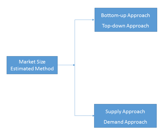
Bottom-up & top-down approach, supply & demand approach are the most important method which is used by HDIN Research to estimate the market size.
1)Top-down & Bottom-up Approach
Top-down approach uses a general market size figure and determines the percentage that the objective market represents.
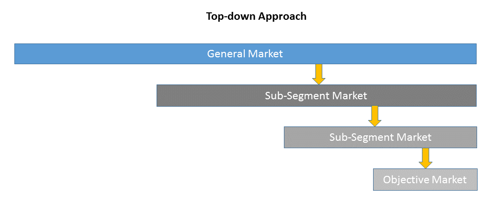
Bottom-up approach size the objective market by collecting the sub-segment information.

2)Supply & Demand Approach
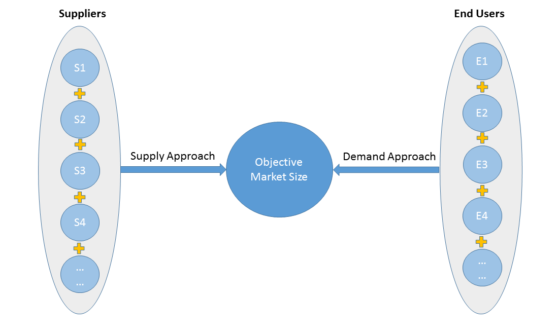
Supply approach is based on assessments of the size of each competitor supplying the objective market.
Demand approach combine end-user data within a market to estimate the objective market size. It is sometimes referred to as bottom-up approach.
- Forecasting Methodology
- Numerous factors impacting the market trend are considered for forecast model:
- New technology and application in the future;
- New project planned/under contraction;
- Global and regional underlying economic growth;
- Threatens of substitute products;
- Industry expert opinion;
- Policy and Society implication.
- Analysis Tools
1)PEST Analysis
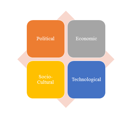
PEST Analysis is a simple and widely used tool that helps our client analyze the Political, Economic, Socio-Cultural, and Technological changes in their business environment.
- Benefits of a PEST analysis:
- It helps you to spot business opportunities, and it gives you advanced warning of significant threats.
- It reveals the direction of change within your business environment. This helps you shape what you’re doing, so that you work with change, rather than against it.
- It helps you avoid starting projects that are likely to fail, for reasons beyond your control.
- It can help you break free of unconscious assumptions when you enter a new country, region, or market; because it helps you develop an objective view of this new environment.
2)Porter’s Five Force Model Analysis
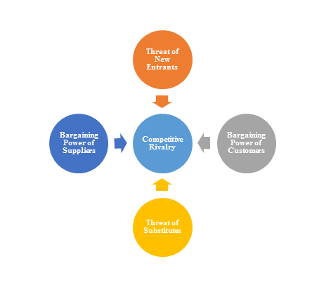
The Porter’s Five Force Model is a tool that can be used to analyze the opportunities and overall competitive advantage. The five forces that can assist in determining the competitive intensity and potential attractiveness within a specific area.
- Threat of New Entrants: Profitable industries that yield high returns will attract new firms.
- Threat of Substitutes: A substitute product uses a different technology to try to solve the same economic need.
- Bargaining Power of Customers: the ability of customers to put the firm under pressure, which also affects the customer's sensitivity to price changes.
- Bargaining Power of Suppliers: Suppliers of raw materials, components, labor, and services (such as expertise) to the firm can be a source of power over the firm when there are few substitutes.
- Competitive Rivalry: For most industries the intensity of competitive rivalry is the major determinant of the competitiveness of the industry.
3)Value Chain Analysis
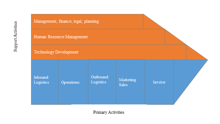
Value chain analysis is a tool to identify activities, within and around the firm and relating these activities to an assessment of competitive strength. Value chain can be analyzed by primary activities and supportive activities. Primary activities include: inbound logistics, operations, outbound logistics, marketing & sales, service. Support activities include: technology development, human resource management, management, finance, legal, planning.
4)SWOT Analysis
SWOT analysis is a tool used to evaluate a company's competitive position by identifying its strengths, weaknesses, opportunities and threats. The strengths and weakness is the inner factor; the opportunities and threats are the external factor. By analyzing the inner and external factors, the analysis can provide the detail information of the position of a player and the characteristics of the industry.
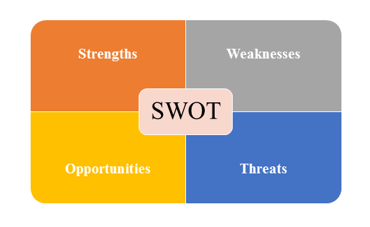
- Strengths describe what the player excels at and separates it from the competition
- Weaknesses stop the player from performing at its optimum level.
- Opportunities refer to favorable external factors that the player can use to give it a competitive advantage.
- Threats refer to factors that have the potential to harm the player.
- Data Sources
| Primary Sources | Secondary Sources |
|---|---|
| Face to face/Phone Interviews with market participants, such as: Manufactures; Distributors; End-users; Experts. Online Survey |
Government/International Organization Data: Annual Report/Presentation/Fact Book Internet Source Information Industry Association Data Free/Purchased Database Market Research Report Book/Journal/News |