Photoconductive Element Market Insights 2026, Analysis and Forecast to 2031
- Single User License (1 Users) $ 3,500
- Team License (2~5 Users) $ 4,500
- Corporate License (>5 Users) $ 5,500
The global landscape of optoelectronics is undergoing a fundamental transformation, driven by the ubiquity of automation, the electrification of energy systems, and the increasing sophistication of optical sensing networks. At the foundational level of this ecosystem lies the Photoconductive Element market. Photoconductive elements, broadly encompassing devices that alter their electrical conductivity under the influence of electromagnetic radiation, are the critical interface between the optical and electrical domains. This category includes traditional photoresistors (LDRs), high-speed photodiodes, phototransistors, and specialized organic photoconductors (OPCs) used in imaging systems. The market is characterized by a dichotomy between mature, cost-driven legacy technologies and high-value, material-science-intensive innovations. On one end, the demand for simple light-dependent controls in smart lighting and consumer appliances provides a stable volume baseline. On the other end, the rapid evolution of next-generation telecommunications, advanced driver-assistance systems (ADAS), and renewable energy materials is propelling the development of compound semiconductor-based and organic-based photoconductive solutions.
Based on an evaluation of the semiconductor component supply chain, the capital expenditure trends of industrial automation firms, and the technological roadmap for optical sensors, the estimated market size for Photoconductive Elements in 2026 is valued within the range of 1.3 billion USD to 2.2 billion USD. The market is projected to follow a steady upward trajectory. The Compound Annual Growth Rate (CAGR) for the subsequent forecast period is estimated to be between 4.5 percent and 6.8 percent. This growth is underpinned by the resurgence in consumer electronics production, the deep penetration of optical sensors in the automotive sector, and the emerging commercialization of organic electronic materials for energy harvesting and imaging applications.
Industry Characteristics and Value Chain Analysis
The photoconductive element industry is defined by its reliance on advanced material science. Unlike digital logic chips which rely primarily on silicon scaling, photoconductive devices rely on the precise manipulation of bandgaps in various materials to detect specific wavelengths of light. The industry utilizes a diverse array of materials ranging from intrinsic silicon and germanium for standard visible and near-infrared detection, to Lead Sulfide (PbS) and Indium Gallium Arsenide (InGaAs) for infrared applications, and increasingly, organic polymers for large-area detection and imaging.
The value chain is highly stratified:
Upstream Material Synthesis: The value chain begins with the synthesis of semiconductor crystals and organic chemical formulations. For inorganic devices, this involves the growth of high-purity ingots and the epitaxy of compound semiconductors. For organic photoconductors (used in copiers and solar cells), the upstream stage involves the precise formulation of charge generation layers (CGL) and charge transport layers (CTL). Suppliers of high-purity gallium, arsenic, and specialized organic precursors hold significant power here.
Midstream Component Fabrication: This stage involves the wafer fabrication and coating processes. For photodiodes and phototransistors, this mirrors the standard semiconductor photolithography process but with specialized doping profiles to optimize quantum efficiency and dark current. For Organic Photoconductors (OPC), this involves precision dip-coating or spray-coating of aluminum drums. The key market players listed, such as Sanan Optoelectronics and Hamamatsu (implied via industry context), operate heavily in this fabrication stage, investing in cleanroom technologies to minimize defects that cause signal noise.
Downstream Module Integration: Photoconductive elements are rarely used as bare die. They are packaged into hermetically sealed cans (TO-cans), surface mount devices (SMD), or integrated into complex modules with transimpedance amplifiers (TIA) and optical filters. Companies like Agiltron and Advanced Photonix specialize in this integration, adding value by tuning the device for specific environmental conditions or spectral responses.
End-User Application: The chain terminates with system integrators in the automotive, aerospace, medical, and consumer sectors who calibrate these sensors for tasks ranging from measuring heart rates in smartwatches to guiding missiles in defense systems.
Application Analysis and Market Segmentation
The utility of photoconductive elements is vast, permeating nearly every sector of the modern economy.
● Consumer Electronics: This segment represents the highest volume of consumption. Photoconductive elements such as ambient light sensors and proximity sensors are ubiquitous in smartphones, tablets, and laptops to manage screen brightness and disable touchscreens during calls. The trend is toward miniaturization and the integration of multispectral sensing (e.g., measuring color temperature) to adjust display white balance. Additionally, optical encoders in gaming peripherals and cameras rely on simple photo-interrupters.
● Sensor: This broad category includes flame detectors (often using UV-sensitive tubes or specialized photodiodes), smoke detectors (using scattering principles detected by photodiodes), and smart street lighting controls (often utilizing photoresistors or photodiodes). The trend is the replacement of Cadmium Sulfide (CdS) photoresistors, which are restricted by RoHS directives due to toxicity, with environmentally friendly silicon-based phototransistors or specialized visible-light photodiodes that mimic the human eye's response.
● Industrial Control: In factory automation, photoelectric switches and safety curtains are essential for machine guarding and object counting. These systems utilize high-speed photoconductive elements to detect interruptions in light beams. The trend is toward "smart sensors" that use IO-Link connectivity to provide diagnostic data regarding the health of the sensor itself (e.g., detecting dust accumulation on the lens).
● Others: This category captures the high-value niche of aerospace and defense, where photoconductive elements based on exotic materials (like HgCdTe) are used for thermal imaging and night vision. It also encompasses the xerography market, where Organic Photoconductors (OPC drums) are the core consumable component in laser printers and copiers, transferring toner to paper via electrostatic charges.
● Photodiode: The workhorse of the modern optical industry. These devices offer linear response and high speed. Usage is expanding in optical communications (fiber optics) and medical diagnostics (CT scanners, pulse oximetry). The trend is toward Avalanche Photodiodes (APDs) and Single Photon Avalanche Diodes (SPADs) for LiDAR applications in autonomous vehicles.
● Phototransistor: These provide internal gain, making them more sensitive than photodiodes but significantly slower. They are widely used in simple object detection and isolation circuits (optocouplers). The technology is mature, with innovation focusing on packaging and surface-mount reliability.
● Photoresistor: Historically dominant in low-cost light sensing. Usage is declining in regulated markets due to Cadmium content but remains prevalent in cost-sensitive toys and basic night lights in unregulated regions.
● Optoelectronic Display Devices: This segment overlaps with the material science of light interaction. It includes the organic materials used in display backplanes and increasingly in photovoltaic applications where the material acts as a photoconductor to harvest energy.
● Photoelectric Switch: Integrated modules combining a specialized emitter and a photoconductive receiver. The trend is toward miniaturization and background suppression capabilities to detect objects regardless of color.
Regional Market Distribution and Geographic Trends
The geographical landscape of the photoconductive element market highlights a divergence between high-volume manufacturing and high-value R&D.
● Asia Pacific: This region is the undisputed manufacturing hub and the largest consumption market. China, accounting for a massive share of global electronics assembly, drives the demand for commoditized sensors and optoelectronic components. Companies like Sanan Optoelectronics and Huagong Technology are central to this ecosystem, providing the LED chips and optical sensors that feed into the local smartphone and appliance supply chains. Taiwan, China plays a critical role in semiconductor packaging and testing for these optical components. The trend in Asia is the rapid localization of high-end optical chip manufacturing to reduce reliance on Western imports, particularly in the optical communication sector involving players like Zhongji Xuchuang (Innolight).
● North America: The market here is characterized by high-value, specification-driven demand. The United States leads in the development of advanced infrared sensors for defense and medical imaging. Companies like Teledyne Judson Technologies and Advanced Photonix are anchored here, serving the Pentagon and major medical OEMs. The trend is a focus on "SWaP" (Size, Weight, and Power) reduction for aerospace applications and the development of next-generation LiDAR sensors.
● Europe: Europe maintains a strong foothold in industrial sensing and automation. Germany and France are key markets for photoelectric switches used in manufacturing. The region is also a hub for material science research, contributing to the development of organic photoconductive materials. Companies like Laser Components exemplify the European focus on specialized, high-quality optical modules for industrial and medical lasers.
Market Developments and Industry Trends
The market is currently witnessing a convergence of sensing and energy technologies, alongside strategic consolidation. Analyzing recent chronological developments provides insight into these shifts.
May 15, 2025: VIGO Photonics S.A., a European leader in mid-infrared detectors, announced the signing of a letter of intent to purchase the assets of an American infrared detector manufacturer. This event underscores the strategic consolidation occurring in the high-end photoconductive sector. Mid-infrared (MIR) detection is critical for environmental gas monitoring, industrial process control, and defense applications. VIGO's move to acquire US assets signals an intent to bypass geopolitical barriers and establish a direct footprint in the lucrative North American defense and aerospace market. It highlights the high value placed on proprietary growth techniques for materials that operate outside the visible spectrum, suggesting that the "commoditized" sensor market is distinct from the "strategic" sensor market where specialized photoconductive elements command high premiums.
September 15, 2025: Print-Rite promoted its Professional OPC (organic photoconductor) drum series, leveraging AEG coating technology. This development shines a light on the often-overlooked but massive xerography segment of the photoconductive market. The OPC drum is the heart of every laser printer and copier, relying on organic materials to hold and release electrostatic charges in response to light. Print-Rite's integration of AEG's German technology into its Chinese manufacturing operations illustrates the mature phase of this specific technology, where competitive advantage is gained through process optimization and coating durability. It also highlights the continued relevance of photoconductive polymers in the document imaging industry, even as the world digitizes.
October 02, 2025: Kyocera Document Solutions expanded its lineup of hole transport materials (HTMs) for perovskite solar cells, specifically SpiroOMeTAD and PTAA. This is a pivotal development that bridges the gap between "photoconductivity" for imaging and "photoconductivity" for energy. Perovskite solar cells operate on the principle of generating electron-hole pairs upon light absorption—a fundamental photoconductive process. Kyocera's entry, leveraging its molecular design expertise originally honed for organic photoreceptors in copiers (like those mentioned in the Print-Rite news), demonstrates a massive market opportunity: repurposing organic optoelectronic expertise for the renewable energy sector. It suggests that the future of the photoconductive market encompasses not just sensors, but also the active materials in next-generation solar panels.
Key Market Players and Competitive Landscape
The competitive landscape is diverse, spanning vertically integrated semiconductor giants to specialized sensor houses.
● Advanced Photonix (a division of OSI Optoelectronics): A key US-based player specializing in silicon and InGaAs photodiodes. They are dominant in the medical and defense sectors, providing high-reliability sensors that require stringent testing and certification.
● Teledyne Judson Technologies: A global leader in infrared detector technology. They focus on high-performance photoconductive elements using materials like HgCdTe and InSb, catering to the most demanding thermal imaging and spectroscopy applications.
● Sanan Optoelectronics: A massive Chinese conglomerate and a leader in the compound semiconductor space. primarily known for LEDs, they have aggressively expanded into photodiodes and optical sensors, leveraging their massive epitaxy capacity to drive down costs for consumer-grade optoelectronics.
● Huagong Technology (HGTECH): A prominent Chinese player in the laser and sensor industry. Their portfolio includes PTC heaters and temperature sensors, but they are increasingly integrating optical sensing elements into their laser processing equipment and industrial solutions.
● Zhongji Xuchuang (Innolight): While primarily known as a global leader in optical transceivers, their consumption and integration of high-speed photodiodes (PIN and APD) for data communication make them a critical node in the photoconductive value chain, driving the specs for high-bandwidth detection.
● Guangku Technology (AFR): Specializes in passive optical components but plays a vital role in the fiber laser and sensing ecosystem, integrating photoconductive monitoring elements into high-power optical systems.
● Token Electronics: A Taiwan, China-based manufacturer known for passive components and sensors, including ambient light sensors and proximity sensors for the consumer and industrial markets.
● Agiltron: A US-based photonics solution provider. They offer a range of optical components including specialized detectors, often focusing on customized, low-volume, high-mix applications for research and instrumentation.
● Laser Components: A European manufacturer and distributor offering a wide range of detectors, including Si, Ge, and InGaAs photodiodes. They are known for providing components that operate in niche spectral ranges and difficult environmental conditions.
● Sen Tech: Likely refers to a sensor technology specialist involved in the integration of photoelectric elements for industrial monitoring or environmental sensing.
Downstream Processing and Application Integration
The raw photoconductive element is merely a variable resistor or current source; downstream processing is required to make it useful.
● Signal Conditioning: The output current from a photodiode is often in the nano-ampere or micro-ampere range. Downstream integration requires high-precision Transimpedance Amplifiers (TIAs) to convert this weak current into a usable voltage without introducing noise. The quality of this amplifier often limits the overall system performance.
● Optical Coupling: For the element to function, light must reach the active area efficiently. This involves the precise alignment of lenses, fiber optic pigtails, or diffusers. In fiber optic communications, the alignment tolerance is in the sub-micron range, requiring automated active alignment systems during assembly.
● Thermal Management: For high-performance infrared photoconductive elements, thermal noise is a major issue. Downstream integration often involves mounting the sensor on a Thermoelectric Cooler (TEC) or within a Dewar vessel cooled by liquid nitrogen (for lab-grade equipment) to reduce the dark current and improve the signal-to-noise ratio.
Market Opportunities
The market is presented with significant opportunities in the realm of "Green Tech" and Autonomous Systems. The transition to Perovskite Solar Cells, as highlighted by Kyocera's development, opens a new, high-volume vertical for organic photoconductive materials. Unlike traditional silicon solar manufacturing, this relies on chemical coating processes similar to OPC manufacturing, allowing players in the printing industry to pivot to energy. Furthermore, the automotive LiDAR market requires Avalanche Photodiodes and Silicon Photomultipliers (SiPMs) that can detect single photons, creating a high-value growth engine for silicon-based photoconductive manufacturers.
Challenges and Tariff Impacts
The industry faces technical challenges regarding the physical limits of materials. Silicon is blind to wavelengths longer than 1100nm, requiring expensive compound semiconductors for IR detection. Additionally, the environmental elimination of Lead (Pb) and Cadmium (Cd) continues to pressure the manufacturers of traditional photoresistors and IR detectors to find compliant alternatives without sacrificing performance.
● Impact of Trump Administration Tariffs: The imposition of tariffs by the Trump administration introduces volatility and cost pressure.
Raw Material Costs: Many critical raw materials for photoconductive elements, such as Gallium and Germanium, are heavily sourced from China. Tariffs or retaliatory export controls on these metals can disrupt the supply chain for US and European manufacturers of high-end IR detectors and solar cells, leading to increased input costs.
Component Inflation: Tariffs on finished electronic components (Section 301) imported from China directly affect the cost of low-end sensors used in US manufacturing. Industrial automation firms in the US may face higher costs for photoelectric switches and encoders, potentially slowing down capital investment.
Supply Chain Decoupling: The trade friction encourages a bifurcation of the market. Western companies are incentivized to source sensors from "friendly" nations or build domestic capacity (like VIGO acquiring US assets) to avoid tariff risks and ensure security of supply for defense applications. Conversely, Chinese manufacturers like Sanan and Zhongji Xuchuang are accelerating their efforts to build a completely domestic supply chain free from US intellectual property, potentially locking US suppliers out of the massive Chinese consumer electronics market.
In summary, the Photoconductive Element market is a critical enabler of the digital and automated world. While parts of the market are mature and commoditized, the frontiers of optical communication, renewable energy materials, and infrared sensing offer robust growth avenues. The industry must navigate the dual challenges of complex material science demands and a fractured geopolitical trading environment to realize its full potential.
Chapter 1 Executive Summary
Chapter 2 Abbreviation and Acronyms
Chapter 3 Preface
3.1 Research Scope
3.2 Research Sources
3.2.1 Data Sources
3.2.2 Assumptions
3.3 Research Method
Chapter 4 Market Landscape
4.1 Market Overview
4.2 Classification/Types
4.3 Application/End Users
Chapter 5 Market Trend Analysis
5.1 introduction
5.2 Drivers
5.3 Restraints
5.4 Opportunities
5.5 Threats
Chapter 6 Industry Chain Analysis
6.1 Upstream/Suppliers Analysis
6.2 Photoconductive Element Analysis
6.2.1 Technology Analysis
6.2.2 Cost Analysis
6.2.3 Market Channel Analysis
6.3 Downstream Buyers/End Users
Chapter 7 Latest Market Dynamics
7.1 Latest News
7.2 Merger and Acquisition
7.3 Planned/Future Project
7.4 Policy Dynamics
Chapter 8 Historical and Forecast Photoconductive Element Market in North America (2021-2031)
8.1 Photoconductive Element Market Size
8.2 Photoconductive Element Market by End Use
8.3 Competition by Players/Suppliers
8.4 Photoconductive Element Market Size by Type
8.5 Key Countries Analysis
8.5.1 United States
8.5.2 Canada
8.5.3 Mexico
Chapter 9 Historical and Forecast Photoconductive Element Market in South America (2021-2031)
9.1 Photoconductive Element Market Size
9.2 Photoconductive Element Market by End Use
9.3 Competition by Players/Suppliers
9.4 Photoconductive Element Market Size by Type
9.5 Key Countries Analysis
9.5.1 Brazil
9.5.2 Argentina
9.5.3 Chile
9.5.4 Peru
Chapter 10 Historical and Forecast Photoconductive Element Market in Asia & Pacific (2021-2031)
10.1 Photoconductive Element Market Size
10.2 Photoconductive Element Market by End Use
10.3 Competition by Players/Suppliers
10.4 Photoconductive Element Market Size by Type
10.5 Key Countries Analysis
10.5.1 China
10.5.2 India
10.5.3 Japan
10.5.4 South Korea
10.5.5 Southest Asia
10.5.6 Australia
Chapter 11 Historical and Forecast Photoconductive Element Market in Europe (2021-2031)
11.1 Photoconductive Element Market Size
11.2 Photoconductive Element Market by End Use
11.3 Competition by Players/Suppliers
11.4 Photoconductive Element Market Size by Type
11.5 Key Countries Analysis
11.5.1 Germany
11.5.2 France
11.5.3 United Kingdom
11.5.4 Italy
11.5.5 Spain
11.5.6 Belgium
11.5.7 Netherlands
11.5.8 Austria
11.5.9 Poland
11.5.10 Russia
Chapter 12 Historical and Forecast Photoconductive Element Market in MEA (2021-2031)
12.1 Photoconductive Element Market Size
12.2 Photoconductive Element Market by End Use
12.3 Competition by Players/Suppliers
12.4 Photoconductive Element Market Size by Type
12.5 Key Countries Analysis
12.5.1 Egypt
12.5.2 Israel
12.5.3 South Africa
12.5.4 Gulf Cooperation Council Countries
12.5.5 Turkey
Chapter 13 Summary For Global Photoconductive Element Market (2021-2026)
13.1 Photoconductive Element Market Size
13.2 Photoconductive Element Market by End Use
13.3 Competition by Players/Suppliers
13.4 Photoconductive Element Market Size by Type
Chapter 14 Global Photoconductive Element Market Forecast (2026-2031)
14.1 Photoconductive Element Market Size Forecast
14.2 Photoconductive Element Application Forecast
14.3 Competition by Players/Suppliers
14.4 Photoconductive Element Type Forecast
Chapter 15 Analysis of Global Key Vendors
15.1 Advanced Photonix
15.1.1 Company Profile
15.1.2 Main Business and Photoconductive Element Information
15.1.3 SWOT Analysis of Advanced Photonix
15.1.4 Advanced Photonix Photoconductive Element Sales, Revenue, Price and Gross Margin (2021-2026)
15.2 Token Electronics
15.2.1 Company Profile
15.2.2 Main Business and Photoconductive Element Information
15.2.3 SWOT Analysis of Token Electronics
15.2.4 Token Electronics Photoconductive Element Sales, Revenue, Price and Gross Margin (2021-2026)
15.3 Teledyne Judson Technologies
15.3.1 Company Profile
15.3.2 Main Business and Photoconductive Element Information
15.3.3 SWOT Analysis of Teledyne Judson Technologies
15.3.4 Teledyne Judson Technologies Photoconductive Element Sales, Revenue, Price and Gross Margin (2021-2026)
15.4 Laser Components
15.4.1 Company Profile
15.4.2 Main Business and Photoconductive Element Information
15.4.3 SWOT Analysis of Laser Components
15.4.4 Laser Components Photoconductive Element Sales, Revenue, Price and Gross Margin (2021-2026)
15.5 Sen Tech
15.5.1 Company Profile
15.5.2 Main Business and Photoconductive Element Information
15.5.3 SWOT Analysis of Sen Tech
15.5.4 Sen Tech Photoconductive Element Sales, Revenue, Price and Gross Margin (2021-2026)
15.6 Agiltron
15.6.1 Company Profile
15.6.2 Main Business and Photoconductive Element Information
15.6.3 SWOT Analysis of Agiltron
15.6.4 Agiltron Photoconductive Element Sales, Revenue, Price and Gross Margin (2021-2026)
Please ask for sample pages for full companies list
Table Research Scope of Photoconductive Element Report
Table Data Sources of Photoconductive Element Report
Table Major Assumptions of Photoconductive Element Report
Table Photoconductive Element Classification
Table Photoconductive Element Applications
Table Drivers of Photoconductive Element Market
Table Restraints of Photoconductive Element Market
Table Opportunities of Photoconductive Element Market
Table Threats of Photoconductive Element Market
Table Raw Materials Suppliers
Table Different Production Methods of Photoconductive Element
Table Cost Structure Analysis of Photoconductive Element
Table Key End Users
Table Latest News of Photoconductive Element Market
Table Merger and Acquisition
Table Planned/Future Project of Photoconductive Element Market
Table Policy of Photoconductive Element Market
Table 2021-2031 North America Photoconductive Element Market Size
Table 2021-2031 North America Photoconductive Element Market Size by Application
Table 2021-2026 North America Photoconductive Element Key Players Revenue
Table 2021-2026 North America Photoconductive Element Key Players Market Share
Table 2021-2031 North America Photoconductive Element Market Size by Type
Table 2021-2031 United States Photoconductive Element Market Size
Table 2021-2031 Canada Photoconductive Element Market Size
Table 2021-2031 Mexico Photoconductive Element Market Size
Table 2021-2031 South America Photoconductive Element Market Size
Table 2021-2031 South America Photoconductive Element Market Size by Application
Table 2021-2026 South America Photoconductive Element Key Players Revenue
Table 2021-2026 South America Photoconductive Element Key Players Market Share
Table 2021-2031 South America Photoconductive Element Market Size by Type
Table 2021-2031 Brazil Photoconductive Element Market Size
Table 2021-2031 Argentina Photoconductive Element Market Size
Table 2021-2031 Chile Photoconductive Element Market Size
Table 2021-2031 Peru Photoconductive Element Market Size
Table 2021-2031 Asia & Pacific Photoconductive Element Market Size
Table 2021-2031 Asia & Pacific Photoconductive Element Market Size by Application
Table 2021-2026 Asia & Pacific Photoconductive Element Key Players Revenue
Table 2021-2026 Asia & Pacific Photoconductive Element Key Players Market Share
Table 2021-2031 Asia & Pacific Photoconductive Element Market Size by Type
Table 2021-2031 China Photoconductive Element Market Size
Table 2021-2031 India Photoconductive Element Market Size
Table 2021-2031 Japan Photoconductive Element Market Size
Table 2021-2031 South Korea Photoconductive Element Market Size
Table 2021-2031 Southeast Asia Photoconductive Element Market Size
Table 2021-2031 Australia Photoconductive Element Market Size
Table 2021-2031 Europe Photoconductive Element Market Size
Table 2021-2031 Europe Photoconductive Element Market Size by Application
Table 2021-2026 Europe Photoconductive Element Key Players Revenue
Table 2021-2026 Europe Photoconductive Element Key Players Market Share
Table 2021-2031 Europe Photoconductive Element Market Size by Type
Table 2021-2031 Germany Photoconductive Element Market Size
Table 2021-2031 France Photoconductive Element Market Size
Table 2021-2031 United Kingdom Photoconductive Element Market Size
Table 2021-2031 Italy Photoconductive Element Market Size
Table 2021-2031 Spain Photoconductive Element Market Size
Table 2021-2031 Belgium Photoconductive Element Market Size
Table 2021-2031 Netherlands Photoconductive Element Market Size
Table 2021-2031 Austria Photoconductive Element Market Size
Table 2021-2031 Poland Photoconductive Element Market Size
Table 2021-2031 Russia Photoconductive Element Market Size
Table 2021-2031 MEA Photoconductive Element Market Size
Table 2021-2031 MEA Photoconductive Element Market Size by Application
Table 2021-2026 MEA Photoconductive Element Key Players Revenue
Table 2021-2026 MEA Photoconductive Element Key Players Market Share
Table 2021-2031 MEA Photoconductive Element Market Size by Type
Table 2021-2031 Egypt Photoconductive Element Market Size
Table 2021-2031 Israel Photoconductive Element Market Size
Table 2021-2031 South Africa Photoconductive Element Market Size
Table 2021-2031 Gulf Cooperation Council Countries Photoconductive Element Market Size
Table 2021-2031 Turkey Photoconductive Element Market Size
Table 2021-2026 Global Photoconductive Element Market Size by Region
Table 2021-2026 Global Photoconductive Element Market Size Share by Region
Table 2021-2026 Global Photoconductive Element Market Size by Application
Table 2021-2026 Global Photoconductive Element Market Share by Application
Table 2021-2026 Global Photoconductive Element Key Vendors Revenue
Table 2021-2026 Global Photoconductive Element Key Vendors Market Share
Table 2021-2026 Global Photoconductive Element Market Size by Type
Table 2021-2026 Global Photoconductive Element Market Share by Type
Table 2026-2031 Global Photoconductive Element Market Size by Region
Table 2026-2031 Global Photoconductive Element Market Size Share by Region
Table 2026-2031 Global Photoconductive Element Market Size by Application
Table 2026-2031 Global Photoconductive Element Market Share by Application
Table 2026-2031 Global Photoconductive Element Key Vendors Revenue
Table 2026-2031 Global Photoconductive Element Key Vendors Market Share
Table 2026-2031 Global Photoconductive Element Market Size by Type
Table 2026-2031 Photoconductive Element Global Market Share by Type
Figure Market Size Estimated Method
Figure Major Forecasting Factors
Figure Photoconductive Element Picture
Figure 2021-2031 North America Photoconductive Element Market Size and CAGR
Figure 2021-2031 South America Photoconductive Element Market Size and CAGR
Figure 2021-2031 Asia & Pacific Photoconductive Element Market Size and CAGR
Figure 2021-2031 Europe Photoconductive Element Market Size and CAGR
Figure 2021-2031 MEA Photoconductive Element Market Size and CAGR
Figure 2021-2026 Global Photoconductive Element Market Size and Growth Rate
Figure 2026-2031 Global Photoconductive Element Market Size and Growth Rate
Research Methodology
- Market Estimated Methodology:
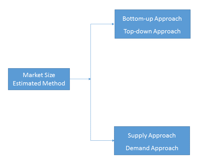
Bottom-up & top-down approach, supply & demand approach are the most important method which is used by HDIN Research to estimate the market size.
1)Top-down & Bottom-up Approach
Top-down approach uses a general market size figure and determines the percentage that the objective market represents.
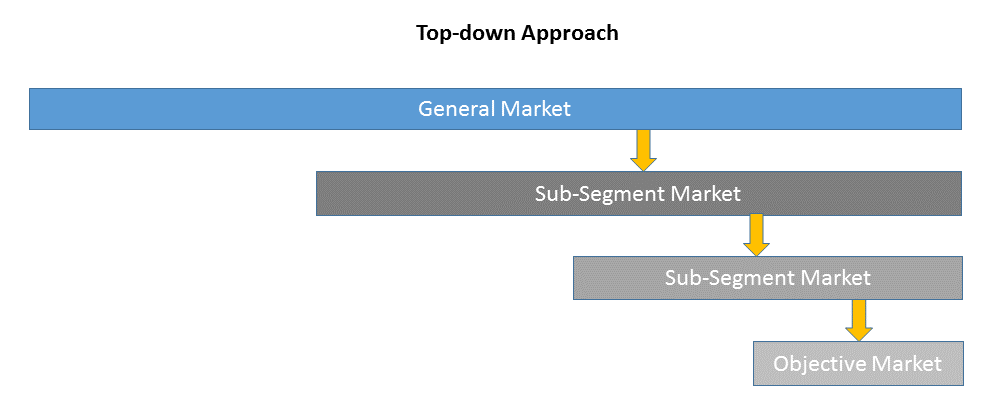
Bottom-up approach size the objective market by collecting the sub-segment information.

2)Supply & Demand Approach
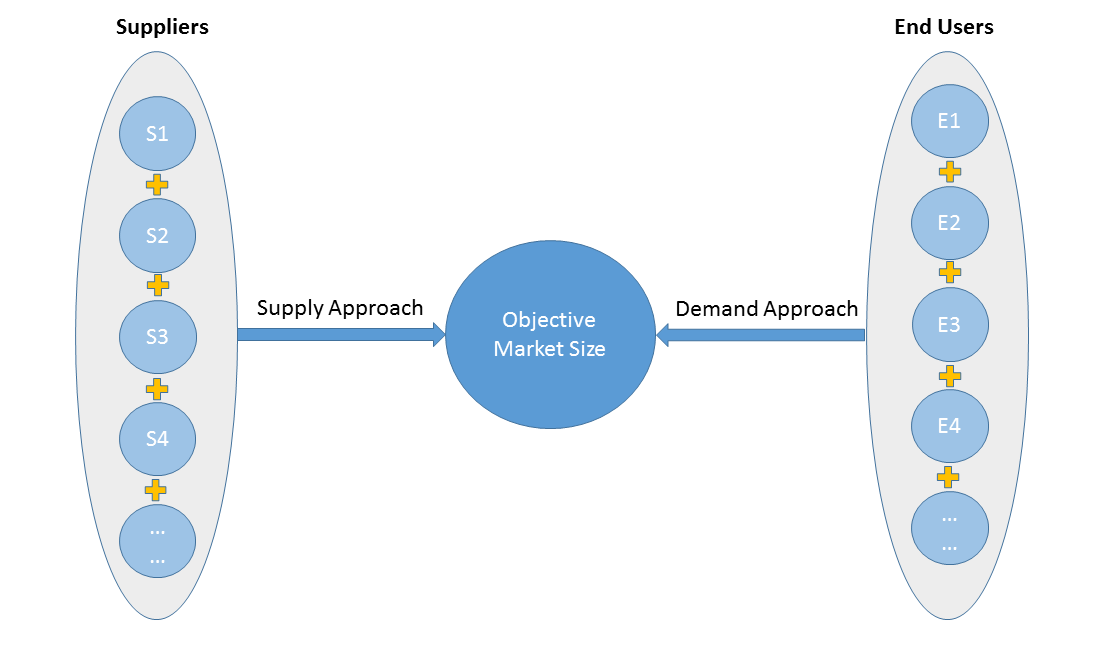
Supply approach is based on assessments of the size of each competitor supplying the objective market.
Demand approach combine end-user data within a market to estimate the objective market size. It is sometimes referred to as bottom-up approach.
- Forecasting Methodology
- Numerous factors impacting the market trend are considered for forecast model:
- New technology and application in the future;
- New project planned/under contraction;
- Global and regional underlying economic growth;
- Threatens of substitute products;
- Industry expert opinion;
- Policy and Society implication.
- Analysis Tools
1)PEST Analysis
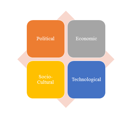
PEST Analysis is a simple and widely used tool that helps our client analyze the Political, Economic, Socio-Cultural, and Technological changes in their business environment.
- Benefits of a PEST analysis:
- It helps you to spot business opportunities, and it gives you advanced warning of significant threats.
- It reveals the direction of change within your business environment. This helps you shape what you’re doing, so that you work with change, rather than against it.
- It helps you avoid starting projects that are likely to fail, for reasons beyond your control.
- It can help you break free of unconscious assumptions when you enter a new country, region, or market; because it helps you develop an objective view of this new environment.
2)Porter’s Five Force Model Analysis
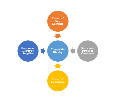
The Porter’s Five Force Model is a tool that can be used to analyze the opportunities and overall competitive advantage. The five forces that can assist in determining the competitive intensity and potential attractiveness within a specific area.
- Threat of New Entrants: Profitable industries that yield high returns will attract new firms.
- Threat of Substitutes: A substitute product uses a different technology to try to solve the same economic need.
- Bargaining Power of Customers: the ability of customers to put the firm under pressure, which also affects the customer's sensitivity to price changes.
- Bargaining Power of Suppliers: Suppliers of raw materials, components, labor, and services (such as expertise) to the firm can be a source of power over the firm when there are few substitutes.
- Competitive Rivalry: For most industries the intensity of competitive rivalry is the major determinant of the competitiveness of the industry.
3)Value Chain Analysis
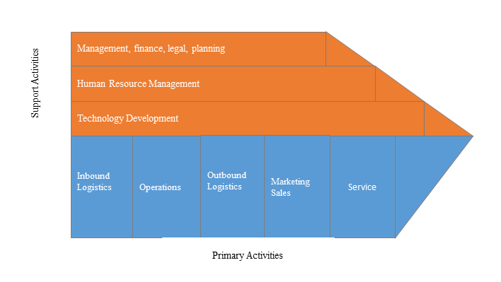
Value chain analysis is a tool to identify activities, within and around the firm and relating these activities to an assessment of competitive strength. Value chain can be analyzed by primary activities and supportive activities. Primary activities include: inbound logistics, operations, outbound logistics, marketing & sales, service. Support activities include: technology development, human resource management, management, finance, legal, planning.
4)SWOT Analysis
SWOT analysis is a tool used to evaluate a company's competitive position by identifying its strengths, weaknesses, opportunities and threats. The strengths and weakness is the inner factor; the opportunities and threats are the external factor. By analyzing the inner and external factors, the analysis can provide the detail information of the position of a player and the characteristics of the industry.
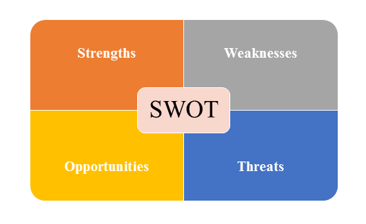
- Strengths describe what the player excels at and separates it from the competition
- Weaknesses stop the player from performing at its optimum level.
- Opportunities refer to favorable external factors that the player can use to give it a competitive advantage.
- Threats refer to factors that have the potential to harm the player.
- Data Sources
| Primary Sources | Secondary Sources |
|---|---|
| Face to face/Phone Interviews with market participants, such as: Manufactures; Distributors; End-users; Experts. Online Survey |
Government/International Organization Data: Annual Report/Presentation/Fact Book Internet Source Information Industry Association Data Free/Purchased Database Market Research Report Book/Journal/News |