Global Automated Laser Debonding Equipment Market Outlook 2026-2031: Advanced Packaging Trends and HBM Drivers
- Single User License (1 Users) $ 3,500
- Team License (2~5 Users) $ 4,500
- Corporate License (>5 Users) $ 5,500
Global Market Overview and Industry Landscape
The Global Automated Laser Debonding Equipment market has established itself as a linchpin in the advanced semiconductor packaging ecosystem. As of 2026, the industry has transitioned from a niche process used primarily in low-volume research to a critical high-volume manufacturing (HVM) step essential for the production of next-generation logic and memory devices. The market size for Automated Laser Debonding Equipment in 2026 is estimated to range between 1.4 billion USD and 2.6 billion USD. The sector is poised for sustained expansion, with a projected Compound Annual Growth Rate (CAGR) estimated between 5.5% and 8.4% through 2031.
Automated laser debonding is a sub-segment of the Temporary Bonding and Debonding (TBDB) market. It involves the use of focused laser energy to detach a processed, ultra-thin device wafer (often less than 50 microns thick) from a rigid carrier wafer. This process is superior to thermal slide or chemical release methods due to its higher throughput, lower mechanical stress, and ability to handle the extreme thermal budgets required in modern backend processing. The primary growth drivers in 2026 are the explosive demand for High Bandwidth Memory (HBM) used in AI accelerators, the proliferation of Fan-Out Wafer Level Packaging (FOWLP), and the increasing complexity of Heterogeneous Integration.
The industry landscape is currently characterized by a technological "arms race" to improve throughput and reduce total cost of ownership (TCO). In mid-2025, significant advancements were made in photonic debonding technologies, a variation of laser debonding that utilizes high-intensity pulsed light. Strategic partnerships, such as the one between Resonac Corporation and PulseForge, Inc., have accelerated the adoption of these high-throughput solutions, aiming to solve the bottlenecks in processing ultra-thin wafers. Furthermore, market leaders like EV Group continue to refine Infrared (IR) laser release technologies, which offer distinct advantages for silicon carrier utilization, a crucial factor for 3D integration schemes.
The market is also witnessing a bifurcation in equipment complexity. At the high end, fully automated clusters capable of handling 300mm wafers (and increasingly 600mm panels) with integrated cleaning and metrology are being deployed in top-tier foundries and OSATs (Outsourced Semiconductor Assembly and Test) facilities. At the mid-tier, more cost-effective standalone units are seeing adoption in the LED and power electronics sectors, particularly for the handling of compound semiconductors like Silicon Carbide (SiC) and Gallium Nitride (GaN).
Value Chain and Supply Chain Structure
The value chain for Automated Laser Debonding Equipment is highly specialized, involving a convergence of optics, precision mechatronics, and materials science.
Upstream: Optical Components and Laser Sources
The upstream segment is dominated by providers of high-power laser sources and precision optics. The choice of laser wavelength—typically Ultraviolet (UV) or Infrared (IR)—dictates the type of debonding process. UV lasers (308nm or 355nm) are commonly used for breaking chemical bonds in adhesive layers, while IR lasers (typically 1064nm) are used to transmit through silicon carriers to heat an absorption layer. Companies like Focuslight Technology play a critical role here, providing beam shaping and optical systems that ensure the laser energy is distributed uniformly across the wafer surface to prevent hotspots and die damage.
Midstream: Equipment Manufacturing and Integration
This is the core of the market, populated by players like SUSS MicroTec, EV Group, and increasingly, Chinese manufacturers like Han's Laser and Delphilaser. These companies integrate the laser engines with robotic wafer handling systems, vision alignment systems, and sophisticated software control. A key trend in the midstream is the collaboration between equipment makers and material suppliers (e.g., Shin-Etsu Chemical). Since the laser debonding process relies heavily on the specific properties of the temporary bonding adhesive and the release layer, integrated solutions where equipment and materials are co-optimized are becoming the industry standard.
Downstream: Semiconductor Manufacturing and Packaging
The end-users are primarily OSATs, Integrated Device Manufacturers (IDMs), and pure-play foundries. In the context of 2026, the downstream demand is heavily skewed towards facilities producing AI chipsets and advanced memory stacks. The reliability of the debonding process is critical; a failure at this stage implies the loss of a fully processed, high-value wafer, making yield the primary purchasing criterion for downstream buyers.
Regional Market Analysis
The geographic distribution of the Automated Laser Debonding Equipment market is closely tied to the global semiconductor manufacturing footprint.
● Asia Pacific
The Asia Pacific region is the dominant market leader, estimated to hold a share between 55% and 65%. This leadership is anchored by Taiwan, China; South Korea; and Mainland China.
Taiwan, China remains the global hub for advanced packaging, driven by the massive capacity of leading foundries handling 2.5D and 3D packaging (such as CoWoS). The demand for laser debonding here is focused on high-end logic integration.
South Korea is a critical market driven by memory giants. The production of HBM, which requires the stacking of 8, 12, or even 16 DRAM dies, necessitates rigorous wafer thinning and handling, directly fueling demand for high-precision laser debonding tools.
China is aggressively expanding its domestic semiconductor equipment capabilities. Local players like Bio-Nano Semi-conductor Equipment and Delphilaser are capturing share in the domestic market, supported by government initiatives to localize the supply chain for advanced packaging.
● North America
North America is estimated to hold a market share between 15% and 20%. While mass manufacturing has largely moved to Asia, the U.S. remains a center for R&D and pilot lines. The resurgence of domestic manufacturing, spurred by legislative incentives, is leading to the construction of new advanced packaging facilities. Companies in this region focus on developing novel bonding/debonding techniques for heterogeneous integration. The adoption of laser debonding for photonics and medical device micro-fabrication is also notable in this region.
● Europe
Europe accounts for an estimated 10% to 15% of the market. The region's strength lies in power electronics (automotive focus) and sensors. The processing of thin SiC and GaN wafers for electric vehicle inverters requires specialized handling solutions where laser debonding plays a role. European equipment manufacturers like SUSS MicroTec and EV Group export significantly to Asia but maintain strong R&D and service hubs within Europe to support local IDMs like Infineon and STMicroelectronics.
● Middle East, Africa (MEA), and South America
These regions collectively hold a smaller share, estimated between 2% and 5%. The market activity is limited compared to the major semiconductor hubs. However, emerging investments in assembly and test facilities in countries like Malaysia (often categorized under APAC but influencing broader flows) and potentially future investments in South America could drive slight growth. Currently, these regions largely utilize legacy thermal debonding equipment, with laser debonding adoption being limited to specific high-value niche applications.
Application and Segmentation Analysis
The application of automated laser debonding is bifurcated into two primary industrial verticals: Semiconductor Packaging and the LED Industry.
● Semiconductor Packaging (Advanced Packaging)
This segment accounts for the majority of market revenue.
3D IC and Through-Silicon Via (TSV): To create vertical interconnects, wafers must be thinned to expose the TSVs. This thinning renders the wafer flexible and fragile, necessitating a carrier wafer. Laser debonding is the preferred method to remove this carrier because it imparts zero mechanical force to the thinned wafer, reducing breakage and stress-induced warping.
Fan-Out Wafer Level Packaging (FOWLP): In "Chip-first" or "Chip-last" processes, molded wafers are often processed on a carrier. Laser debonding allows for high-throughput separation of the reconstituted wafer from the carrier, essential for cost-sensitive mobile applications.
High Bandwidth Memory (HBM): As memory stacks grow higher, the individual dies must be thinner. The HBM manufacturing flow relies heavily on temporary bonding. Recent trends highlight the shift towards hybrid bonding, where laser debonding equipment must operate with extreme cleanliness to prevent particle contamination that would ruin the interconnects.
● LED Industry (Mini/Micro LED)
While traditionally a smaller market than logic/memory, the LED sector is a significant user of Laser Lift-Off (LLO) technology, a variant of laser debonding.
Micro LED Transfer: Manufacturing Micro LED displays involves growing LEDs on a sapphire or GaAs substrate and then transferring them to a backplane. Laser debonding is used to separate the massive arrays of microscopic LEDs from their growth substrate rapidly.
Flexible Displays: The production of flexible OLED and micro-LED displays often involves processing on a rigid glass carrier followed by laser release.
Key Market Players and Company Developments
The competitive landscape is a mix of established European precision engineering firms and rapidly growing Asian equipment manufacturers.
● EV Group (EVG)
EV Group remains a dominant force and a technological trendsetter. In February 2025, the company highlighted its industry-leading IR LayerRelease™ technology at SEMICON Korea. This technology is pivotal because it allows for the use of silicon carriers instead of glass. Silicon carriers are preferred for 3D integration because they have the same Coefficient of Thermal Expansion (CTE) as the device wafer, minimizing alignment errors. EVG’s equipment is widely regarded as the benchmark for HVM in HBM and 3D stacking production lines.
● SUSS MicroTec
A key competitor to EVG, SUSS MicroTec holds a strong position in the advanced packaging market. Their platforms often feature modular designs that allow for easy reconfiguration between different debonding modalities (e.g., UV laser vs. Excimer). SUSS has a strong foothold in the OSAT market and is known for the reliability of its wafer handling robotics, which is crucial when handling thinned wafers post-debonding.
● Shin-Etsu Chemical
While primarily a materials giant, Shin-Etsu plays a unique role. They provide the total solution: the temporary bonding adhesive, the release layer, and the equipment specifications (often developed in partnership or via proprietary systems). Their OD (One-stop Solution for Debonding) systems are highly optimized for their own chemical materials, creating a "lock-in" effect that ensures high yield for customers.
● Han's Laser & Delphilaser
These Chinese manufacturers have moved up the value chain. Originally focused on laser marking and cutting, they have developed sophisticated laser debonding systems for the semiconductor industry. Han's Laser leverages its massive scale in laser source manufacturing to offer cost-competitive solutions. Delphilaser has specialized in solid-state laser processing and has gained traction in the domestic Chinese market for Micro LED and power semiconductor debonding applications.
● Bio-Nano Semi-conductor Equipment
An emerging player focusing on specialized packaging equipment. They are increasingly active in the domestic Chinese market, targeting mid-tier packaging houses that require reliable debonding solutions without the premium price tag of European tools.
● Focuslight Technology
Focuslight is critical in the optical subsystem domain. Their beam shaping technologies (such as micro-optic homogenizers) are often integrated into the debonding systems of other OEMs. By transforming Gaussian laser beams into uniform "Top-Hat" profiles, they ensure that the debonding energy is applied evenly across the wafer, preventing localized stress or incomplete release.
● Resonac Corporation (Strategic Partnership context)
The partnership between Resonac and PulseForge (June 2025) signifies the entry of new photonic debonding technologies. Resonac (formerly Showa Denko) brings material science expertise, while PulseForge brings high-intensity pulsed light technology. This collaboration aims to introduce a process that is faster than traditional laser scanning, potentially disrupting the throughput standards of the market.
Market Opportunities
● Commercialization of MicroLED Displays
The transition of MicroLED from prototype to mass production represents a massive opportunity. The transfer of millions of LEDs requires extremely fast debonding techniques. Equipment that can perform "Mass Transfer" via laser processes with high yield will see significant demand from the consumer electronics and automotive display sectors.
● Panel-Level Packaging (PLP)
To reduce costs, the industry is exploring moving from round wafers (300mm) to large rectangular panels (e.g., 600mm x 600mm). This increases the number of chips per process step. Current laser debonding equipment is being scaled up to handle these large panels. Manufacturers who can maintain uniformity and focus depth over these large areas will capture the emerging PLP market.
● AI-Driven Process Control
The integration of Artificial Intelligence into debonding equipment offers a path to higher yields. AI can analyze real-time sensor data during the laser scan to predict and adjust for variations in the release layer thickness or wafer warpage. Equipment featuring "Self-Correcting" capabilities will be highly attractive to high-volume manufacturers.
Market Challenges
● Managing Wafer Warpage
As wafers become thinner (approaching 20 microns or less), they tend to warp significantly once removed from the carrier. This makes subsequent handling and cleaning extremely difficult. The challenge for equipment makers is not just the debonding itself, but the integrated handling of the "floppy" wafer immediately after separation. Failure to manage warpage leads to wafer breakage and massive financial loss.
● High Capital Expenditure (CAPEX)
Laser debonding systems are significantly more expensive than mechanical or thermal slide debonding tools. The laser sources (particularly high-power UV or specialized IR) are costly components. For cost-sensitive applications like analog or legacy logic packaging, the ROI of laser debonding can be difficult to justify, limiting its adoption to the high end of the market.
● Residue Cleaning
After laser debonding, a carbonized residue or adhesive remnant often remains on the device wafer. This requires a subsequent cleaning step (usually chemical or plasma ashing). This adds to the process time and complexity. Developing "cleaner" release layers and laser processes that minimize residue is a constant technical challenge for the industry.
Future Outlook
The Automated Laser Debonding Equipment market is entering a phase of maturity and diversification. By 2031, laser debonding is expected to be the standard for all sub-50-micron wafer processing. The market will likely see a convergence of bonding and debonding steps into unified clusters to minimize footprint and contamination risks.
Technologically, the shift towards IR laser debonding is expected to gain momentum as it enables the use of standard silicon carriers, which are compatible with existing fab automation. Furthermore, the rise of "chiplets" will drive the need for more granular, die-level debonding solutions in addition to full-wafer processes. The sustained investment in AI infrastructure and the unavoidable physics of 3D scaling ensure that the ability to temporarily bond and safely debond ultra-thin silicon will remain a cornerstone of the semiconductor manufacturing value chain.
1.1 Study Scope 1
1.2 Research Methodology 2
1.2.1 Data Sources 3
1.2.2 Assumptions 4
1.3 Abbreviations and Acronyms 6
Chapter 2 Market Dynamics and Industry Trends 7
2.1 Market Drivers: Demand for 2.5D/3D Advanced Packaging 7
2.2 Market Constraints: High Equipment Maintenance and Complexity 9
2.3 Technological Trends: Transition from Thermal to Laser Debonding 11
2.4 Laser Source Innovations: Excimer vs. Solid-State Lasers 13
2.5 Patent Analysis and Intellectual Property Landscape 15
Chapter 3 Global Automated Laser Debonding Equipment Market by Type 18
3.1 Excimer Laser Debonding Systems 18
3.1.1 Market Volume and Size (2021-2026) 19
3.2 Solid-State Laser Debonding Systems 21
3.2.1 Market Volume and Size (2021-2026) 22
3.3 Comparative Analysis of Debonding Throughput and Efficiency 24
Chapter 4 Global Automated Laser Debonding Equipment Market by Application 26
4.1 Semiconductor Packaging 26
4.1.1 Fan-out Wafer Level Packaging (FOWLP) Trends 27
4.1.2 Market Volume and Size (2021-2026) 28
4.2 LED Industry 30
4.2.1 Micro-LED and Mini-LED Transfer Applications 31
4.2.2 Market Volume and Size (2021-2026) 32
Chapter 5 Global Automated Laser Debonding Equipment Market by Key Regions 35
5.1 North America 35
5.1.1 United States 37
5.2 Europe 39
5.2.1 Germany 40
5.2.2 Netherlands 41
5.3 Asia-Pacific 43
5.3.1 China 44
5.3.2 Japan 45
5.3.3 South Korea 46
5.3.4 Taiwan (China) 47
5.4 Rest of the World 49
Chapter 6 Production Process and Value Chain Analysis 51
6.1 Automated Laser Debonding Equipment Manufacturing Workflow 51
6.2 Laser Source Integration and Optical Path Calibration 53
6.3 Upstream Component Analysis (Lasers, Stages, Sensors) 55
6.4 Value Chain Analysis 57
Chapter 7 Global Automated Laser Debonding Equipment Import and Export 60
7.1 Global Export Trends by Key Regions 60
7.2 Global Import Trends by Key Regions 62
Chapter 8 Global Market Competitive Landscape 64
8.1 Global Revenue Share by Key Player (2021-2026) 64
8.2 Market Concentration Ratio 66
8.3 Recent Developments: M&A and Strategic Alliances 68
Chapter 9 Key Company Profiles 70
9.1 Shin-Etsu Chemical 70
9.1.1 Company Overview and Product Portfolio 70
9.1.2 SWOT Analysis 71
9.1.3 Shin-Etsu Laser Debonding Sales, Price, Cost and Gross Profit Margin (2021-2026) 72
9.1.4 Strategic R&D in Materials-Equipment Synergy 73
9.2 SUSS MicroTec 74
9.2.1 Company Overview and Product Portfolio 74
9.2.2 SWOT Analysis 75
9.2.3 SUSS Laser Debonding Sales, Price, Cost and Gross Profit Margin (2021-2026) 77
9.3 EV Group 79
9.3.1 Company Overview and Product Portfolio 79
9.3.2 SWOT Analysis 80
9.3.3 EVG Laser Debonding Sales, Price, Cost and Gross Profit Margin (2021-2026) 82
9.4 Delphilaser 84
9.4.1 Company Overview and Product Portfolio 84
9.4.2 SWOT Analysis 85
9.4.3 Delphilaser Laser Debonding Sales, Price, Cost and Gross Profit Margin (2021-2026) 87
9.5 Han's Laser 89
9.5.1 Company Overview 89
9.5.2 Han's Laser Debonding Sales, Price, Cost and Gross Profit Margin (2021-2026) 91
9.6 Bio-Nano Semiconductor Equipment 93
9.6.1 Company Overview 93
9.6.2 Bio-Nano Laser Debonding Sales, Price, Cost and Gross Profit Margin (2021-2026) 95
9.7 Focuslight Technology 97
9.7.1 Company Overview 97
9.7.2 Focuslight Laser Debonding Sales, Price, Cost and Gross Profit Margin (2021-2026) 99
Chapter 10 Global Automated Laser Debonding Equipment Market Forecast (2027-2031) 101
10.1 Global Market Size and Volume Forecast 101
10.2 Forecast by Type (2027-2031) 103
10.3 Forecast by Application (2027-2031) 105
10.4 Forecast by Key Regions (2027-2031) 107
Chapter 11 Conclusion and Industry Summary 110
Table 2. Key Manufacturers Production Capacity (Units) 2026 52
Table 3. Cost Breakdown of a Standard Laser Debonding System 56
Table 4. Global Revenue Share by Key Player (2021-2026) 65
Table 5. Shin-Etsu Laser Debonding Sales, Price, Cost and Gross Profit Margin (2021-2026) 72
Table 6. SUSS Laser Debonding Sales, Price, Cost and Gross Profit Margin (2021-2026) 77
Table 7. EVG Laser Debonding Sales, Price, Cost and Gross Profit Margin (2021-2026) 82
Table 8. Delphilaser Laser Debonding Sales, Price, Cost and Gross Profit Margin (2021-2026) 87
Table 9. Han's Laser Laser Debonding Sales, Price, Cost and Gross Profit Margin (2021-2026) 91
Table 10. Bio-Nano Laser Debonding Sales, Price, Cost and Gross Profit Margin (2021-2026) 95
Table 11. Focuslight Laser Debonding Sales, Price, Cost and Gross Profit Margin (2021-2026) 99
Table 12. Global Market Volume Forecast by Type (Units) 2027-2031 104
Table 13. Global Market Size Forecast by Application (M USD) 2027-2031 106
Table 14. Global Market Size Forecast by Key Regions (M USD) 2027-2031 109
Figure 1. Automated Laser Debonding Equipment Research Methodology 4
Figure 2. Global Automated Laser Debonding Equipment Market Size (M USD) 2021-2026 8
Figure 3. Global Automated Laser Debonding Equipment Market Volume (Units) 2021-2026 12
Figure 4. Market Share by Laser Type in 2026 18
Figure 5. Excimer Laser Debonding Growth Trajectory (2021-2026) 20
Figure 6. Global Market Size Share by Application in 2026 27
Figure 7. Semiconductor Packaging Segment Consumption Trend 29
Figure 8. LED Industry Segment Revenue Growth (2021-2026) 33
Figure 9. North America Market Revenue (M USD) 2021-2026 36
Figure 10. Asia-Pacific Market Revenue (M USD) 2021-2026 43
Figure 11. China Automated Laser Debonding Equipment Market Dynamics 44
Figure 12. Industry Value Chain Map 58
Figure 13. Global Export Share by Region 2026 61
Figure 14. Global Market Revenue Share by Key Player 2026 65
Figure 15. Shin-Etsu Laser Debonding Market Share (2021-2026) 72
Figure 16. SUSS Laser Debonding Market Share (2021-2026) 77
Figure 17. EVG Laser Debonding Market Share (2021-2026) 82
Figure 18. Delphilaser Laser Debonding Market Share (2021-2026) 87
Figure 19. Han's Laser Laser Debonding Market Share (2021-2026) 91
Figure 20. Bio-Nano Laser Debonding Market Share (2021-2026) 95
Figure 21. Focuslight Laser Debonding Market Share (2021-2026) 99
Figure 22. Global Automated Laser Debonding Equipment Market Size Forecast (2027-2031) 102
Figure 23. Regional Market Forecast Opportunity Map 2031 108
Research Methodology
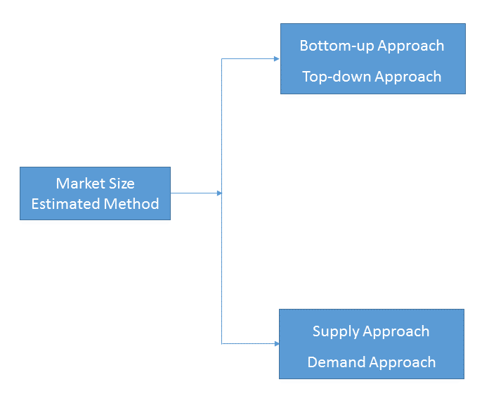
- Market Estimated Methodology:
Bottom-up & top-down approach, supply & demand approach are the most important method which is used by HDIN Research to estimate the market size.
1)Top-down & Bottom-up Approach
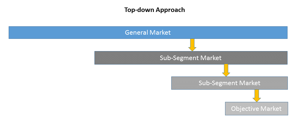
Top-down approach uses a general market size figure and determines the percentage that the objective market represents.
Bottom-up approach size the objective market by collecting the sub-segment information.

2)Supply & Demand Approach
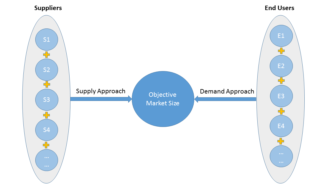
Supply approach is based on assessments of the size of each competitor supplying the objective market.
Demand approach combine end-user data within a market to estimate the objective market size. It is sometimes referred to as bottom-up approach.
- Forecasting Methodology
- Numerous factors impacting the market trend are considered for forecast model:
- New technology and application in the future;
- New project planned/under contraction;
- Global and regional underlying economic growth;
- Threatens of substitute products;
- Industry expert opinion;
- Policy and Society implication.
- Analysis Tools
1)PEST Analysis
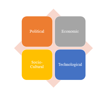
PEST Analysis is a simple and widely used tool that helps our client analyze the Political, Economic, Socio-Cultural, and Technological changes in their business environment.
- Benefits of a PEST analysis:
- It helps you to spot business opportunities, and it gives you advanced warning of significant threats.
- It reveals the direction of change within your business environment. This helps you shape what you’re doing, so that you work with change, rather than against it.
- It helps you avoid starting projects that are likely to fail, for reasons beyond your control.
- It can help you break free of unconscious assumptions when you enter a new country, region, or market; because it helps you develop an objective view of this new environment.
2)Porter’s Five Force Model Analysis
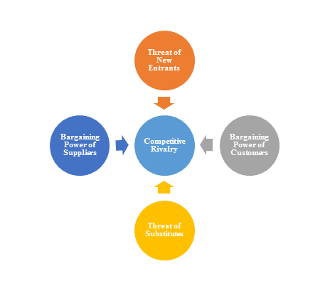
The Porter’s Five Force Model is a tool that can be used to analyze the opportunities and overall competitive advantage. The five forces that can assist in determining the competitive intensity and potential attractiveness within a specific area.
- Threat of New Entrants: Profitable industries that yield high returns will attract new firms.
- Threat of Substitutes: A substitute product uses a different technology to try to solve the same economic need.
- Bargaining Power of Customers: the ability of customers to put the firm under pressure, which also affects the customer's sensitivity to price changes.
- Bargaining Power of Suppliers: Suppliers of raw materials, components, labor, and services (such as expertise) to the firm can be a source of power over the firm when there are few substitutes.
- Competitive Rivalry: For most industries the intensity of competitive rivalry is the major determinant of the competitiveness of the industry.
3)Value Chain Analysis
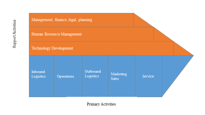
Value chain analysis is a tool to identify activities, within and around the firm and relating these activities to an assessment of competitive strength. Value chain can be analyzed by primary activities and supportive activities. Primary activities include: inbound logistics, operations, outbound logistics, marketing & sales, service. Support activities include: technology development, human resource management, management, finance, legal, planning.
4)SWOT Analysis
SWOT analysis is a tool used to evaluate a company's competitive position by identifying its strengths, weaknesses, opportunities and threats. The strengths and weakness is the inner factor; the opportunities and threats are the external factor. By analyzing the inner and external factors, the analysis can provide the detail information of the position of a player and the characteristics of the industry.
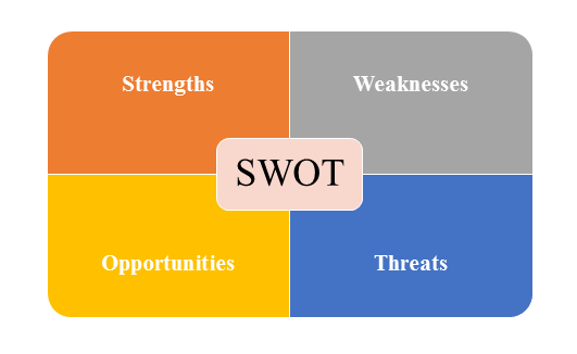
- Strengths describe what the player excels at and separates it from the competition
- Weaknesses stop the player from performing at its optimum level.
- Opportunities refer to favorable external factors that the player can use to give it a competitive advantage.
- Threats refer to factors that have the potential to harm the player.
- Data Sources
| Primary Sources | Secondary Sources |
|---|---|
| Face to face/Phone Interviews with market participants, such as: Manufactures; Distributors; End-users; Experts. Online Survey |
Government/International Organization Data: Annual Report/Presentation/Fact Book Internet Source Information Industry Association Data Free/Purchased Database Market Research Report Book/Journal/News |