Global Epoxy Resin Molding Compounds for Semiconductor Market: Advanced Packaging Trends, Value Chain, and Industry Forecast
- Single User License (1 Users) $ 3,500
- Team License (2~5 Users) $ 4,500
- Corporate License (>5 Users) $ 5,500
The global semiconductor manufacturing industry is characterized by an unyielding pursuit of miniaturization, power efficiency, and enhanced performance. Within the intricate and highly specialized backend assembly and testing supply chain, Epoxy Resin Molding Compounds (EMC) operate as an absolutely indispensable foundational material. Whenever consumers interact with modern electronics, the ubiquitous black plastic enclosures encapsulating the internal microchips—such as Central Processing Units (CPUs), memory modules, and specialized sensors—are predominantly manufactured using EMC. The fundamental mission of this sophisticated material is to provide uncompromising mechanical protection to the incredibly fragile semiconductor die and the microscopic wire bonds that connect it to the lead frame or substrate. Furthermore, EMC serves to hermetically seal the delicate integrated circuits, completely isolating them from external moisture, airborne dust, and severe chemical corrosion, while simultaneously acting as a critical thermal bridge to dissipate the intense heat generated during chip operation.
As a mission-critical consumable in the semiconductor backend packaging process, the Epoxy Resin Molding Compound market is defined by astronomically high technological barriers to entry and exceptionally protracted customer certification cycles. The formulation of EMC is not a mere blending of chemicals; it represents a highly guarded equilibrium of polymer chemistry, thermodynamics, and materials science. Because the failure of the molding compound inevitably results in the catastrophic failure of the entire semiconductor package, Outsourced Semiconductor Assembly and Test (OSAT) companies and Integrated Device Manufacturers (IDMs) require years of rigorous reliability testing before qualifying a new EMC supplier.
Consequently, the global EMC market currently exhibits a highly concentrated, oligopolistic structure. It is a sector deeply entrenched and locked down by a formidable "Japanese Legion." Global top-tier enterprises, the vast majority of which are headquartered in Japan, currently control well over 60 percent of the total market share. In this fiercely competitive yet exclusive arena, the proprietary accumulation of highly secretive material recipes and the capacity for seamless, joint research and development with leading semiconductor foundries constitute an insurmountable moat against new entrants. Despite these barriers, the market is expanding rapidly due to the explosive growth of artificial intelligence, high-performance computing, and automotive electrification.
The global Epoxy Resin Molding Compounds for Semiconductor market is projected to reach an estimated market size ranging from 2.46 to 6.45 Billion USD by the year 2026. Looking forward into the subsequent decade, the market is forecasted to maintain a steady and resilient Compound Annual Growth Rate (CAGR) of 4.7% to 5.5% through 2031. This growth trajectory underscores the material's critical role in enabling the next generation of advanced semiconductor packaging technologies.
Regional Market Analysis
The geographical distribution of the Epoxy Resin Molding Compound market is inextricably linked to the global footprints of OSAT facilities, semiconductor foundries, and the overarching geopolitical strategies governing localized semiconductor supply chains.
• Asia-Pacific Market Trends and Projections
The Asia-Pacific region is the undisputed epicenter of the global semiconductor packaging industry, acting as the primary consumption and production hub for the EMC market. The region is projected to experience robust growth, with an estimated CAGR ranging from 5.5% to 6.5%. Taiwan, China remains a critical pillar in this ecosystem, hosting the world's most advanced semiconductor foundries and top-tier OSATs. The demand for ultra-high-end EMC in Taiwan, China is surging, driven by advanced heterogeneous integration and high-bandwidth memory packaging for AI accelerators. Mainland China represents the fastest-growing consumption market, heavily fueled by aggressive national policies aimed at semiconductor self-sufficiency. As domestic OSATs rapidly expand their capacities in mature and advanced nodes, the push for localized supply chains is creating massive opportunities for domestic EMC manufacturers to substitute imported materials. South Korea, dominated by memory chip titans, relies heavily on specialized EMC for multi-chip stacking in DRAM and NAND flash memory. Japan, while maintaining a strong domestic OSAT presence, acts primarily as the technological brain trust and primary exporter of premium EMC to the rest of the Asia-Pacific.
• North America Market Trends and Projections
The North American market, dominated by the United States, is undergoing a profound structural renaissance, with an estimated growth rate of 4.0% to 5.0%. Historically, the U.S. focused heavily on fabless chip design, outsourcing assembly to Asia. However, recent geopolitical shifts and massive legislative frameworks, such as the CHIPS and Science Act, are aggressively incentivizing the reshoring of both front-end fabrication and back-end advanced packaging facilities. As major semiconductor companies build advanced packaging research and development centers and commercial OSAT facilities on American soil, the domestic demand for high-performance and advanced packaging EMC is set to rise significantly. Furthermore, North America leads the global development of Artificial Intelligence and high-performance computing architectures, directly driving the R&D specifications for next-generation, low-warpage molding compounds.
• Europe Market Trends and Projections
The European market is deeply integrated with the region's powerhouse automotive and industrial manufacturing sectors, projecting an estimated growth rate of 3.5% to 4.5%. Europe is home to leading global IDMs specializing in power electronics, automotive microcontrollers, and industrial sensors. The rapid transition toward electric vehicles (EVs) across the European Union is a primary growth catalyst. Automotive semiconductors, particularly those utilizing Silicon Carbide (SiC) and Gallium Nitride (GaN) technologies, operate at significantly higher temperatures and voltages than standard consumer chips. Consequently, the European market exhibits an outsized demand for specialized, high-temperature, and high-reliability automotive-grade Epoxy Resin Molding Compounds that can withstand severe thermal cycling and extreme environmental stress.
• South America Market Trends and Projections
The South American market represents a steady, albeit smaller, emerging landscape, with an estimated growth rate of 2.5% to 3.5%. The market here is predominantly driven by consumer electronics assembly and localized manufacturing initiatives in countries like Brazil and Mexico (often categorized broadly within Latin American supply chains). The demand focuses primarily on basic and mid-range EMC for legacy chip packaging and consumer appliance components, though the trend of nearshoring electronics manufacturing to serve the North American market is beginning to stimulate demand for more advanced semiconductor materials in the region.
• Middle East and Africa (MEA) Market Trends and Projections
The MEA region occupies a niche segment of the global EMC market, with an estimated growth rate of 2.0% to 3.0%. The market is anchored by specific high-tech corridors, such as the advanced semiconductor R&D and fabrication facilities located in Israel. The broader African continent is gradually seeing an increase in electronic assembly and telecommunications infrastructure, which will incrementally drive long-term demand for packaged semiconductors. The Gulf nations' investments in smart city infrastructure and technology diversification are also laying the groundwork for future advanced electronics manufacturing.
Application and Type Classification Analysis
The EMC market is highly segmented, driven by the diverse physical architectures of semiconductor packages and the rigorous reliability requirements of their end-use applications.
• Basic EMC Type Trends
Basic Epoxy Molding Compounds are traditionally utilized for legacy packaging formats such as Dual In-line Packages (DIP), Small Outline Packages (SOP), and Quad Flat Packages (QFP). These compounds typically feature standard spherical silica fillers and traditional epoxy resin backbones. While their relative share of the overall market revenue is gradually shrinking in favor of advanced materials, Basic EMC continues to account for massive volume consumption. This sustained demand is driven by the vast array of commodity electronics, basic analog ICs, and discrete components that do not require cutting-edge miniaturization but demand extreme cost-efficiency and proven, long-term reliability.
• High-Performance EMC Type Trends
High-Performance EMC bridges the gap between legacy packages and the bleeding edge of semiconductor technology. These compounds are engineered for more complex architectures like Quad Flat No-leads (QFN) and standard Ball Grid Arrays (BGA). The prevailing trend in this category is the urgent need for enhanced thermal conductivity and ultra-low moisture absorption. As consumer electronics become thinner and more powerful, the chips within them generate more heat in confined spaces. High-Performance EMC utilizes sophisticated multi-modal silica filler distributions (blending different sizes of microscopic silica spheres) to maximize filler loading, thereby significantly improving the compound's ability to pull heat away from the die while preventing delamination during the high-temperature solder reflow process (the "popcorn effect").
• Advanced Packaging EMC Type Trends
Advanced Packaging EMC represents the most lucrative, technologically demanding, and fastest-growing segment of the market. This category supports revolutionary packaging techniques such as Fan-Out Wafer Level Packaging (FOWLP), 2.5D/3D Integrated Circuits (ICs), Chiplets, and High Bandwidth Memory (HBM). In these architectures, multiple silicon dies are densely packed and interconnected on a single substrate or silicon interposer. The critical trend here is absolute warpage control. Because the silicon dies and the EMC have different Coefficients of Thermal Expansion (CTE), temperature changes during manufacturing can cause the entire package to warp, destroying microscopic interconnections. Advanced Packaging EMC requires exotic, ultra-low CTE formulations, exceptionally fine filler particles (to flow into microscopic gaps between stacked chips, often referred to as Molded Underfill or MUF), and low-alpha-particle-emitting materials to prevent soft errors in dense memory arrays.
• Consumer Electronics Application Trends
Consumer electronics, encompassing smartphones, personal computers, tablets, and smart wearables, remains the largest application segment by volume. The relentless consumer demand for thinner, lighter, and more battery-efficient devices forces semiconductor manufacturers to shrink package sizes continually. This drives the demand for specialized molding compounds that can flow into incredibly thin mold cavities (often less than a millimeter thick) without leaving voids or causing wire sweep (the bending of delicate gold or copper wires during the injection of the EMC).
• Automotive Application Trends
The automotive sector is the fastest-growing application segment, fundamentally transformed by the advent of Electric Vehicles (EVs) and Advanced Driver Assistance Systems (ADAS). Automotive-grade semiconductors must achieve zero-defect reliability and comply with stringent AEC-Q100 standards, as chip failure can lead to fatal accidents. The transition from internal combustion engines to EV powertrains relies heavily on power modules handling hundreds of volts and operating at ambient temperatures exceeding 175 degrees Celsius. EMC formulated for automotive applications must feature revolutionary high glass transition temperatures (Tg), extreme resistance to thermal shock, and immunity to high-voltage tracking.
• Industrial Application Trends
Industrial applications demand ruggedized semiconductor packaging capable of surviving harsh factory environments. Chips used in industrial automation, robotics, high-power motor drives, and renewable energy inverters (solar and wind) require EMC that offers exceptional high-voltage insulation and resistance to prolonged thermal stress. The trend is moving toward highly thermally conductive molding compounds that extend the operational lifespan of power discrete components in continuous, heavy-duty industrial cycles.
• Aerospace and Others Application Trends
In the aerospace and defense sectors, semiconductor packaging faces the most extreme environmental challenges on Earth and beyond. EMC used in these applications must endure violent vibrational shock, extreme temperature fluctuations from cryogenic cold to atmospheric reentry heat, and intense cosmic radiation. Specialized radiation-hardened molding compounds are developed for these niche, low-volume, but astronomically high-value applications. Other emerging applications include IoT edge devices and 5G/6G telecommunications infrastructure, which require advanced EMC with ultra-low dielectric constants to minimize signal loss in high-frequency radio transmissions.
Industry Chain and Value Chain Structure
The economic realities and formidable entry barriers of the EMC market are best understood through the lens of its highly specialized, deeply integrated industry and value chain.
• Upstream Raw Materials
The upstream segment involves the synthesis and processing of fundamental chemical building blocks. An EMC formulation typically consists of 70% to 90% inorganic fillers (predominantly spherical silica), 5% to 15% epoxy resins (the binder), phenolic resins (curing agents), and minor but critical additives including flame retardants, adhesion promoters (silane coupling agents), carbon black (for laser marking and light shielding), and mold release agents. The silica filler is arguably the most critical upstream component. Achieving the perfect spherical shape, absolute chemical purity, and precise particle size distribution requires highly advanced combustion and classification technologies. The supply of ultra-pure spherical silica is tightly controlled by a few specialized materials companies, meaning EMC manufacturers must secure robust upstream partnerships to guarantee the quality and consistency of their final product.
• Midstream Formulation and Manufacturing
The midstream encompasses the core EMC manufacturers. The value addition in this phase does not come from complex chemical synthesis, but rather from unparalleled expertise in formulation and mechanical processing. Developing an EMC recipe is highly empirical, requiring years of trial and error to balance contradictory properties (e.g., maximizing filler content for low CTE while maintaining enough fluidity to mold without damaging wires). The manufacturing process involves precision weighing, dry blending, and high-temperature melt-kneading through twin-screw extruders. The compound is then rapidly cooled, crushed into granules, and tableted. Because the material begins to cross-link (cure) at room temperature, the entire midstream manufacturing, storage, and logistics chain must be strictly temperature-controlled (often requiring continuous cold-chain logistics), adding significant complexity and cost to the value chain.
• Downstream OSAT and IDM Integration
The downstream segment consists of the semiconductor packaging facilities operated by OSATs and IDMs. This is where the ultimate value of the EMC is realized. The relationship between midstream EMC suppliers and downstream semiconductor manufacturers is uniquely symbiotic. Because new semiconductor architectures (like 3D packaging) require entirely novel material properties, EMC suppliers station their chemical engineers directly inside the foundries. They engage in joint R&D years before a new chip reaches commercial mass production. This deep, embedded collaboration forms the core "moat" of the industry; once a specific EMC formulation is written into a chip's manufacturing Process of Record (POR), the OSAT will not change the supplier for the entire lifecycle of that product due to the astronomical risks and costs of re-qualification.
Company Information and Competitive Landscape
The global EMC competitive landscape is heavily skewed toward legacy Japanese chemical and materials conglomerates. These enterprises leveraged their early integration with Japan's booming consumer electronics industry in the 1980s to build an insurmountable lead in polymer formulation data and global OSAT relationships.
• Sumitomo Bakelite
Sumitomo Bakelite stands as the undisputed global hegemon in the Epoxy Resin Molding Compound market. Controlling a massive plurality of the global market share, the company sets the technological benchmark for the entire industry. Their dominance is rooted in a vast library of proprietary resin formulations and an unparalleled global manufacturing footprint that places their compounding facilities in close proximity to major OSAT hubs worldwide. Sumitomo Bakelite commands absolute leadership in premium segments, particularly in ultra-low warpage compounds required for cutting-edge smartphones, automotive power modules, and advanced heterogeneous integration packaging.
• Resonac (formerly Showa Denko and Hitachi Chemical)
Following the integration of Hitachi Chemical into Showa Denko to form Resonac, the company has solidified its position as a towering giant in semiconductor materials. Resonac possesses deep historical expertise in polymer chemistry and maintains deeply entrenched relationships with top-tier global foundries and IDMs. They are particularly aggressive in developing next-generation advanced packaging materials, pioneering Granular Molding Compounds (GMC) and highly specialized underfills essential for high-density chiplet architectures and AI accelerators.
• KYOCERA Chemical Corporation, Shin-Etsu Chemical, Nitto Denko, and Panasonic
These companies complete the elite "Japanese Legion." KYOCERA leverages its broader expertise in advanced ceramics and electronic components to engineer highly reliable molding compounds. Shin-Etsu Chemical, already a global titan in silicon wafers and silicone materials, provides exceptionally pure EMCs, heavily utilizing their internal mastery of silica and resin synthesis. Nitto Denko and Panasonic continue to provide highly specialized encapsulation solutions, particularly focusing on power electronics, optical sensors, and automotive-grade reliability, reinforcing the collective dominance of Japanese material science in the semiconductor backend.
• KCC and Chang Chun Group
Operating outside of Japan, KCC (South Korea) and Chang Chun Group (Taiwan, China) are highly strategic regional players. KCC benefits immensely from its proximity to and deep integration with South Korea's massive memory semiconductor conglomerates, tailoring its EMC formulations for high-yield DRAM and NAND packaging. Chang Chun Group is a cornerstone of the robust semiconductor supply chain in Taiwan, China. By working closely with the island's world-leading foundries and OSATs, Chang Chun provides critical, high-quality EMC alternatives, ensuring regional supply chain resilience against geopolitical shocks.
• Hysol Huawei Electronics, Jiangsu Huahai, Scienchem, and PhiChem
These enterprises represent the vanguard of mainland China's aggressive push for semiconductor material localization. Hysol Huawei Electronics (historically linked to joint ventures) and Jiangsu Huahai have successfully commercialized large volumes of Basic and High-Performance EMC, capturing significant market share in discrete components, consumer electronics, and mature IC packaging within the domestic Chinese market. Scienchem and PhiChem are heavily investing in intense R&D to breach the advanced packaging fortress. Driven by national strategic mandates and the urgent need of domestic OSATs for secure supply chains, these Chinese companies are rapidly iterating their formulations to compete in Fan-Out, System-in-Package (SiP), and high-end memory applications, serving as the primary engines of import substitution in the APAC region.
Market Opportunities and Challenges
The Epoxy Resin Molding Compound market resides at the absolute frontier of Moore's Law, presenting chemical manufacturers with unprecedented commercial opportunities coupled with severe physical and engineering challenges.
• Market Opportunities
The most explosive opportunity in the current era is the Artificial Intelligence megatrend. AI data centers require massive arrays of High Bandwidth Memory (HBM) and Logic dies packaged closely together using 2.5D interposers (like CoWoS technology). The traditional transfer molding of solid EMC pellets struggles with these massive, ultra-thin package formats. This has birthed highly lucrative sub-markets for Liquid Compression Molding (LCM) materials and Granular Molding Compounds (GMC), which can flow seamlessly over large heterogeneous packages without damaging delicate chiplets. Material suppliers who successfully qualify these advanced formats command exceptional profit margins.
Furthermore, the rapid transition to Silicon Carbide (SiC) in the EV industry presents a massive opportunity. SiC chips can operate at temperatures that physically degrade standard epoxy resins. Developing novel high-Tg (Glass Transition Temperature) EMCs utilizing advanced multi-functional epoxy structures or entirely new polyimide/cyanate ester blends opens a vast, highly profitable frontier in automotive power electronics. Finally, the global geopolitical drive to de-risk and localize semiconductor supply chains creates an unprecedented window of opportunity for non-Japanese manufacturers to gain qualification at major foundries that are actively seeking to diversify their supplier base.
• Market Challenges
The market is counterbalanced by terrifyingly steep technical challenges. In advanced 3D packaging, resolving the Coefficient of Thermal Expansion (CTE) mismatch is the ultimate engineering hurdle. The EMC must perfectly match the thermal expansion rate of the silicon die, the copper pillars, and the organic substrate simultaneously. Any slight deviation results in package warpage, leading to shattered solder joints and dead chips. Achieving this requires loading the compound with up to 90% silica filler while somehow maintaining the viscosity of water during the molding process—a near-impossible paradox in polymer physics.
Additionally, the formidable OSAT qualification barrier remains the primary business challenge. A new EMC supplier must provide years of reliability data, passing thousands of hours of Highly Accelerated Stress Testing (HAST), thermal cycling, and moisture sensitivity level (MSL) testing. Even a single failure in a batch of millions can result in immediate disqualification and immense financial liability, making the market exceptionally hostile to new entrants lacking deep financial reserves and historical data accumulation.
1.1 Study Scope .................... 1
1.2 Research Methodology .................... 2
1.2.1 Data Sources .................... 2
1.2.2 Assumptions .................... 3
1.3 Abbreviations and Acronyms .................... 4
Chapter 2 Global Epoxy Resin Molding Compounds for Semiconductor Market Executive Summary .................... 5
2.1 Executive Summary and Market Overview .................... 5
2.2 Global EMC Capacity, Production, and Market Size (2021-2031) .................... 6
2.3 Major Semiconductor Packaging Demand Trends and Consumption Dynamics .................... 7
2.4 Key Industry Drivers, Challenges, and Technology Drivers .................... 8
Chapter 3 Macroeconomic and Geopolitical Dynamics Analysis .................... 9
3.1 Global Semiconductor Industry Macro Environment Analysis .................... 9
3.2 Geopolitical Conflict Impact Analysis (Including Middle East Crisis Impact) .................... 10
3.3 Semiconductor Material Supply Chain Resilience and Global Logistics Disruptions .................... 11
3.4 Environmental Policies, Flame Retardancy Standards, and Hazardous Substance Directives .................... 12
Chapter 4 Epoxy Resin Molding Compounds Production Technology and Patent Landscape .................... 13
4.1 Advanced Resin Formulation and High Silica Filler Loading Technology .................... 13
4.2 Manufacturing Process for Fan-Out, 2.5D/3D IC, and Heterogeneous Integration EMC .................... 14
4.3 Warpage Control, Low Moisture Absorption, and Thermal Management Optimization .................... 15
4.4 Global Patent Landscape and Technology Development Trends .................... 16
Chapter 5 Global Epoxy Resin Molding Compounds for Semiconductor Market Segmentation by Type .................... 17
5.1 Market Segment Breakdown by Product Type .................... 17
5.1.1 Basic EMC .................... 18
5.1.2 High-Performance EMC .................... 19
5.1.3 Advanced Packaging EMC .................... 20
5.2 Global EMC Capacity, Production, Revenue, and Share by Type (2021-2031) .................... 21
5.3 Price Trend Analysis and Margin Comparison across EMC Product Grades .................... 21
Chapter 6 Global Epoxy Resin Molding Compounds for Semiconductor Market Segmentation by Application .................... 22
6.1 Market Breakdown by Downstream Application Sector .................... 22
6.1.1 Consumer Electronics .................... 22
6.1.2 Automotive .................... 23
6.1.3 Industrial .................... 24
6.1.4 Aerospace .................... 25
6.1.5 Others .................... 25
6.2 Global EMC Consumption Volume and Revenue by Application (2021-2031) .................... 26
6.3 Downstream Penetration Rates and Advanced Packaging Growth Opportunities .................... 26
Chapter 7 Global EMC Production, Capacity, and Import/Export Analysis .................... 27
7.1 Global Production Capacity, Output Volume, and Utilization Rates (2021-2026) .................... 27
7.2 Key Regional Manufacturing Hubs and Supply Distribution .................... 28
7.3 Global Import and Export Trade Dynamics (2021-2026) .................... 29
7.4 Trade Tariffs, Regional Material Autonomy, and Logistics Risks .................... 30
Chapter 8 Regional Epoxy Resin Molding Compounds for Semiconductor Market Analysis .................... 31
8.1 North America Market (Capacity, Production, Consumption, and Revenue) .................... 31
8.1.1 United States .................... 32
8.1.2 Canada .................... 33
8.1.3 Mexico .................... 34
8.2 Europe Market (Capacity, Production, Consumption, and Revenue) .................... 35
8.2.1 Germany .................... 36
8.2.2 France .................... 37
8.2.3 United Kingdom .................... 38
8.2.4 Italy .................... 39
8.2.5 Rest of Europe .................... 40
8.3 Asia-Pacific Market (Capacity, Production, Consumption, and Revenue) .................... 41
8.3.1 China .................... 42
8.3.2 Japan .................... 43
8.3.3 South Korea .................... 44
8.3.4 Southeast Asia .................... 45
8.3.5 India .................... 46
8.3.6 Taiwan (China) .................... 47
8.3.7 Rest of Asia-Pacific .................... 48
8.4 Latin America Market (Capacity, Production, Consumption, and Revenue) .................... 49
8.4.1 Brazil .................... 50
8.4.2 Rest of Latin America .................... 50
8.5 Middle East & Africa Market (Capacity, Production, Consumption, and Revenue) .................... 51
8.5.1 GCC Countries .................... 51
8.5.2 South Africa .................... 51
8.5.3 Rest of Middle East & Africa .................... 51
Chapter 9 Industry Chain Structure, Raw Materials, and Customer Analysis .................... 52
9.1 Upstream Raw Material Supply Chain (Epoxy Resins, Spherical Silica Fillers, Hardeners) .................... 52
9.2 Manufacturing Cost Structure Analysis .................... 53
9.3 Direct Sales Channels and OSAT / IDM Customer Qualification Routes .................... 54
9.4 Key Semiconductor Packaging Customers Analysis .................... 55
Chapter 10 Key Market Players Analysis .................... 57
10.1 Sumitomo Bakelite .................... 57
10.1.1 Company Overview and Core Business .................... 57
10.1.2 SWOT Analysis .................... 58
10.1.3 R&D Investment and Marketing Strategy .................... 58
10.1.4 Epoxy Resin Molding Compounds for Semiconductor Operating Data Analysis .................... 59
10.2 Resonac .................... 61
10.2.1 Company Overview and Core Business .................... 61
10.2.2 SWOT Analysis .................... 62
10.2.3 R&D Investment and Marketing Strategy .................... 62
10.2.4 Epoxy Resin Molding Compounds for Semiconductor Operating Data Analysis .................... 63
10.3 KYOCERA Chemical Corporation .................... 65
10.3.1 Company Overview and Core Business .................... 65
10.3.2 SWOT Analysis .................... 66
10.3.3 R&D Investment and Marketing Strategy .................... 66
10.3.4 Epoxy Resin Molding Compounds for Semiconductor Operating Data Analysis .................... 67
10.4 Shin-Etsu Chemical .................... 69
10.4.1 Company Overview and Core Business .................... 69
10.4.2 SWOT Analysis .................... 70
10.4.3 R&D Investment and Marketing Strategy .................... 70
10.4.4 Epoxy Resin Molding Compounds for Semiconductor Operating Data Analysis .................... 71
10.5 Nitto Denko .................... 73
10.5.1 Company Overview and Core Business .................... 73
10.5.2 SWOT Analysis .................... 74
10.5.3 R&D Investment and Marketing Strategy .................... 74
10.5.4 Epoxy Resin Molding Compounds for Semiconductor Operating Data Analysis .................... 75
10.6 Panasonic .................... 77
10.6.1 Company Overview and Core Business .................... 77
10.6.2 SWOT Analysis .................... 78
10.6.3 R&D Investment and Marketing Strategy .................... 78
10.6.4 Epoxy Resin Molding Compounds for Semiconductor Operating Data Analysis .................... 79
10.7 KCC .................... 81
10.7.1 Company Overview and Core Business .................... 81
10.7.2 SWOT Analysis .................... 82
10.7.3 R&D Investment and Marketing Strategy .................... 82
10.7.4 Epoxy Resin Molding Compounds for Semiconductor Operating Data Analysis .................... 83
10.8 Chang Chun Group .................... 85
10.8.1 Company Overview and Core Business .................... 85
10.8.2 SWOT Analysis .................... 86
10.8.3 R&D Investment and Marketing Strategy .................... 86
10.8.4 Epoxy Resin Molding Compounds for Semiconductor Operating Data Analysis .................... 87
10.9 Hysol Huawei Electronics .................... 89
10.9.1 Company Overview and Core Business .................... 89
10.9.2 SWOT Analysis .................... 90
10.9.3 R&D Investment and Marketing Strategy .................... 90
10.9.4 Epoxy Resin Molding Compounds for Semiconductor Operating Data Analysis .................... 91
10.10 Jiangsu Huahai .................... 93
10.10.1 Company Overview and Core Business .................... 93
10.10.2 SWOT Analysis .................... 94
10.10.3 R&D Investment and Marketing Strategy .................... 94
10.10.4 Epoxy Resin Molding Compounds for Semiconductor Operating Data Analysis .................... 95
10.11 Scienchem .................... 97
10.11.1 Company Overview and Core Business .................... 97
10.11.2 SWOT Analysis .................... 98
10.11.3 R&D Investment and Marketing Strategy .................... 98
10.11.4 Epoxy Resin Molding Compounds for Semiconductor Operating Data Analysis .................... 99
10.12 PhiChem .................... 101
10.12.1 Company Overview and Core Business .................... 101
10.12.2 SWOT Analysis .................... 102
10.12.3 R&D Investment and Marketing Strategy .................... 102
10.12.4 Epoxy Resin Molding Compounds for Semiconductor Operating Data Analysis .................... 103
Chapter 11 Market Competition Dynamics and Share Analysis .................... 105
11.1 Global Market Share Distribution of Leading EMC Vendors (2021-2026) .................... 105
11.2 Industry Concentration Ratio (CR3, CR5, CR10) .................... 106
11.3 Key Strategic Mergers, OSAT Customer Alliances, and Capacity Expansions .................... 107
Chapter 12 Global Epoxy Resin Molding Compounds for Semiconductor Market Forecast (2027-2031) .................... 108
12.1 Global Capacity and Production Forecast by Region (2027-2031) .................... 108
12.2 Global Consumption and Revenue Forecast by Application (2027-2031) .................... 109
12.3 Price and Gross Margin Trends Forecast (2027-2031) .................... 110
Table 2. Global Epoxy Resin Molding Compounds for Semiconductor Market Overview Snapshot (2021, 2026, 2031) .................... 5
Table 3. Key Patents in Semiconductor Encapsulation and Advanced EMC Formulations .................... 16
Table 4. Global Epoxy Resin Molding Compounds for Semiconductor Production Volume by Product Type (2021-2026) .................... 21
Table 5. Global Epoxy Resin Molding Compounds for Semiconductor Revenue by Product Type (2021-2026) .................... 21
Table 6. Global Epoxy Resin Molding Compounds for Semiconductor Selling Price by Type (2021-2026) .................... 21
Table 7. Global Epoxy Resin Molding Compounds for Semiconductor Consumption Volume by Application (2021-2026) .................... 26
Table 8. Global Epoxy Resin Molding Compounds for Semiconductor Revenue by Application (2021-2026) .................... 26
Table 9. Global Epoxy Resin Molding Compounds for Semiconductor Consumption Forecast by Application (2027-2031) .................... 26
Table 10. Global EMC Capacity and Production Volume by Region (2021-2026) .................... 27
Table 11. Global EMC Import Volume by Key Region (2021-2026) .................... 29
Table 12. Global EMC Export Volume by Key Region (2021-2026) .................... 29
Table 13. North America EMC Production, Consumption, and Revenue (2021-2026) .................... 31
Table 14. United States EMC Market Performance (2021-2026) .................... 32
Table 15. Canada EMC Market Performance (2021-2026) .................... 33
Table 16. Mexico EMC Market Performance (2021-2026) .................... 34
Table 17. Europe EMC Production, Consumption, and Revenue (2021-2026) .................... 35
Table 18. Germany EMC Market Performance (2021-2026) .................... 36
Table 19. France EMC Market Performance (2021-2026) .................... 37
Table 20. United Kingdom EMC Market Performance (2021-2026) .................... 38
Table 21. Italy EMC Market Performance (2021-2026) .................... 39
Table 22. Asia-Pacific EMC Production, Consumption, and Revenue (2021-2026) .................... 41
Table 23. China EMC Market Performance (2021-2026) .................... 42
Table 24. Japan EMC Market Performance (2021-2026) .................... 43
Table 25. South Korea EMC Market Performance (2021-2026) .................... 44
Table 26. Southeast Asia EMC Market Performance (2021-2026) .................... 45
Table 27. India EMC Market Performance (2021-2026) .................... 46
Table 28. Taiwan (China) EMC Market Performance (2021-2026) .................... 47
Table 29. Upstream Raw Material Supply Prices and Material Trends .................... 52
Table 30. Major Key OSAT and IDM Semiconductor Customers .................... 55
Table 31. Sumitomo Bakelite Epoxy Resin Molding Compounds for Semiconductor Capacity, Production, Price, Cost and Gross Profit Margin (2021-2026) .................... 59
Table 32. Resonac Epoxy Resin Molding Compounds for Semiconductor Capacity, Production, Price, Cost and Gross Profit Margin (2021-2026) .................... 63
Table 33. KYOCERA Chemical Corporation Epoxy Resin Molding Compounds for Semiconductor Capacity, Production, Price, Cost and Gross Profit Margin (2021-2026) .................... 67
Table 34. Shin-Etsu Chemical Epoxy Resin Molding Compounds for Semiconductor Capacity, Production, Price, Cost and Gross Profit Margin (2021-2026) .................... 71
Table 35. Nitto Denko Epoxy Resin Molding Compounds for Semiconductor Capacity, Production, Price, Cost and Gross Profit Margin (2021-2026) .................... 75
Table 36. Panasonic Epoxy Resin Molding Compounds for Semiconductor Capacity, Production, Price, Cost and Gross Profit Margin (2021-2026) .................... 79
Table 37. KCC Epoxy Resin Molding Compounds for Semiconductor Capacity, Production, Price, Cost and Gross Profit Margin (2021-2026) .................... 83
Table 38. Chang Chun Group Epoxy Resin Molding Compounds for Semiconductor Capacity, Production, Price, Cost and Gross Profit Margin (2021-2026) .................... 87
Table 39. Hysol Huawei Electronics Epoxy Resin Molding Compounds for Semiconductor Capacity, Production, Price, Cost and Gross Profit Margin (2021-2026) .................... 91
Table 40. Jiangsu Huahai Epoxy Resin Molding Compounds for Semiconductor Capacity, Production, Price, Cost and Gross Profit Margin (2021-2026) .................... 95
Table 41. Scienchem Epoxy Resin Molding Compounds for Semiconductor Capacity, Production, Price, Cost and Gross Profit Margin (2021-2026) .................... 99
Table 42. PhiChem Epoxy Resin Molding Compounds for Semiconductor Capacity, Production, Price, Cost and Gross Profit Margin (2021-2026) .................... 103
Table 43. Global EMC Market Share Breakdown by Leading Suppliers (2021-2026) .................... 105
Table 44. Global EMC Capacity and Production Forecast by Region (2027-2031) .................... 108
Table 45. Global EMC Revenue Forecast by Region (2027-2031) .................... 109
Table 46. Global EMC Average Selling Price and Margin Forecast (2027-2031) .................... 110
Figure 1. Global Epoxy Resin Molding Compounds for Semiconductor Revenue and Growth Rate (2021-2031) .................... 6
Figure 2. Global Epoxy Resin Molding Compounds for Semiconductor Capacity and Production Volume (2021-2031) .................... 6
Figure 3. Impact Assessment Matrix of Geopolitical Conflict on Semiconductor Material Supply Chain .................... 10
Figure 4. Manufacturing Process and Silica Filler Loading Flowchart for Semiconductor EMC .................... 14
Figure 5. Global Semiconductor EMC Patent Filing Trend (2021-2026) .................... 16
Figure 6. Global Epoxy Resin Molding Compounds for Semiconductor Market Share by Product Type in 2026 .................... 21
Figure 7. Global Epoxy Resin Molding Compounds for Semiconductor Market Share by Application in 2026 .................... 26
Figure 8. Global EMC Capacity Utilization Rate Trend (2021-2026) .................... 27
Figure 9. Major Global Export Corridors for Semiconductor EMC (2026) .................... 29
Figure 10. North America Epoxy Resin Molding Compounds for Semiconductor Market Size (2021-2031) .................... 31
Figure 11. Europe Epoxy Resin Molding Compounds for Semiconductor Market Size (2021-2031) .................... 35
Figure 12. Asia-Pacific Epoxy Resin Molding Compounds for Semiconductor Market Size (2021-2031) .................... 41
Figure 13. Latin America Epoxy Resin Molding Compounds for Semiconductor Market Size (2021-2031) .................... 49
Figure 14. Middle East & Africa Epoxy Resin Molding Compounds for Semiconductor Market Size (2021-2031) .................... 51
Figure 15. Epoxy Resin Molding Compounds Manufacturing Cost Structure Breakdown .................... 53
Figure 16. Sumitomo Bakelite Epoxy Resin Molding Compounds for Semiconductor Market Share (2021-2026) .................... 59
Figure 17. Resonac Epoxy Resin Molding Compounds for Semiconductor Market Share (2021-2026) .................... 63
Figure 18. KYOCERA Chemical Corporation Epoxy Resin Molding Compounds for Semiconductor Market Share (2021-2026) .................... 67
Figure 19. Shin-Etsu Chemical Epoxy Resin Molding Compounds for Semiconductor Market Share (2021-2026) .................... 71
Figure 20. Nitto Denko Epoxy Resin Molding Compounds for Semiconductor Market Share (2021-2026) .................... 75
Figure 21. Panasonic Epoxy Resin Molding Compounds for Semiconductor Market Share (2021-2026) .................... 79
Figure 22. KCC Epoxy Resin Molding Compounds for Semiconductor Market Share (2021-2026) .................... 83
Figure 23. Chang Chun Group Epoxy Resin Molding Compounds for Semiconductor Market Share (2021-2026) .................... 87
Figure 24. Hysol Huawei Electronics Epoxy Resin Molding Compounds for Semiconductor Market Share (2021-2026) .................... 91
Figure 25. Jiangsu Huahai Epoxy Resin Molding Compounds for Semiconductor Market Share (2021-2026) .................... 95
Figure 26. Scienchem Epoxy Resin Molding Compounds for Semiconductor Market Share (2021-2026) .................... 99
Figure 27. PhiChem Epoxy Resin Molding Compounds for Semiconductor Market Share (2021-2026) .................... 103
Figure 28. Market Share Distribution of Leading Global EMC Manufacturers in 2026 .................... 105
Figure 29. Global Demand Forecast for Semiconductor EMC by Downstream Sector (2027-2031) .................... 109
Research Methodology
- Market Estimated Methodology:
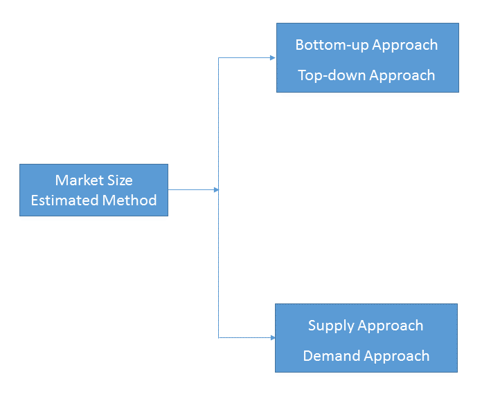
Bottom-up & top-down approach, supply & demand approach are the most important method which is used by HDIN Research to estimate the market size.
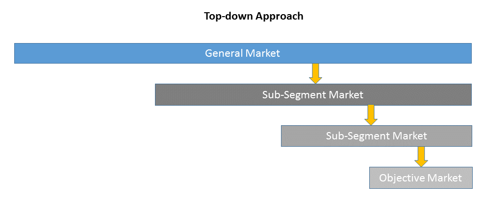
1)Top-down & Bottom-up Approach
Top-down approach uses a general market size figure and determines the percentage that the objective market represents.
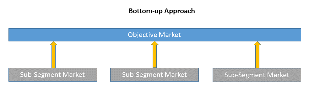
Bottom-up approach size the objective market by collecting the sub-segment information.
2)Supply & Demand Approach
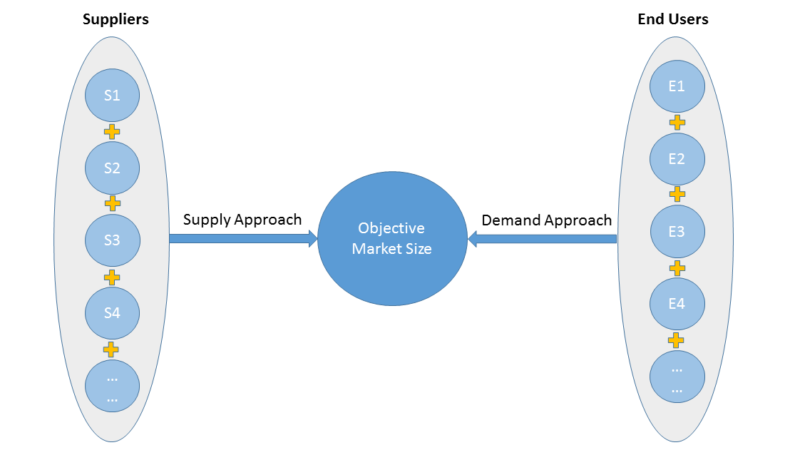
Supply approach is based on assessments of the size of each competitor supplying the objective market.
Demand approach combine end-user data within a market to estimate the objective market size. It is sometimes referred to as bottom-up approach.
- Forecasting Methodology
- Numerous factors impacting the market trend are considered for forecast model:
- New technology and application in the future;
- New project planned/under contraction;
- Global and regional underlying economic growth;
- Threatens of substitute products;
- Industry expert opinion;
- Policy and Society implication.
- Analysis Tools
1)PEST Analysis
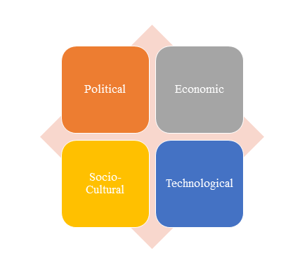
PEST Analysis is a simple and widely used tool that helps our client analyze the Political, Economic, Socio-Cultural, and Technological changes in their business environment.
- Benefits of a PEST analysis:
- It helps you to spot business opportunities, and it gives you advanced warning of significant threats.
- It reveals the direction of change within your business environment. This helps you shape what you’re doing, so that you work with change, rather than against it.
- It helps you avoid starting projects that are likely to fail, for reasons beyond your control.
- It can help you break free of unconscious assumptions when you enter a new country, region, or market; because it helps you develop an objective view of this new environment.
2)Porter’s Five Force Model Analysis
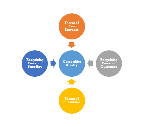
The Porter’s Five Force Model is a tool that can be used to analyze the opportunities and overall competitive advantage. The five forces that can assist in determining the competitive intensity and potential attractiveness within a specific area.
- Threat of New Entrants: Profitable industries that yield high returns will attract new firms.
- Threat of Substitutes: A substitute product uses a different technology to try to solve the same economic need.
- Bargaining Power of Customers: the ability of customers to put the firm under pressure, which also affects the customer's sensitivity to price changes.
- Bargaining Power of Suppliers: Suppliers of raw materials, components, labor, and services (such as expertise) to the firm can be a source of power over the firm when there are few substitutes.
- Competitive Rivalry: For most industries the intensity of competitive rivalry is the major determinant of the competitiveness of the industry.
3)Value Chain Analysis
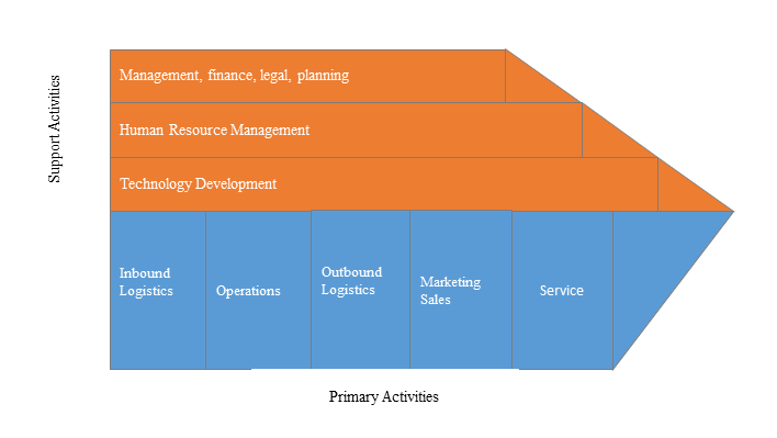
Value chain analysis is a tool to identify activities, within and around the firm and relating these activities to an assessment of competitive strength. Value chain can be analyzed by primary activities and supportive activities. Primary activities include: inbound logistics, operations, outbound logistics, marketing & sales, service. Support activities include: technology development, human resource management, management, finance, legal, planning.
4)SWOT Analysis
SWOT analysis is a tool used to evaluate a company's competitive position by identifying its strengths, weaknesses, opportunities and threats. The strengths and weakness is the inner factor; the opportunities and threats are the external factor. By analyzing the inner and external factors, the analysis can provide the detail information of the position of a player and the characteristics of the industry.
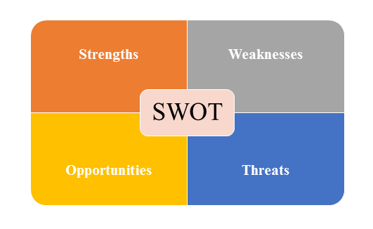
- Strengths describe what the player excels at and separates it from the competition
- Weaknesses stop the player from performing at its optimum level.
- Opportunities refer to favorable external factors that the player can use to give it a competitive advantage.
- Threats refer to factors that have the potential to harm the player.
- Data Sources
| Primary Sources | Secondary Sources |
|---|---|
| Face to face/Phone Interviews with market participants, such as: Manufactures; Distributors; End-users; Experts. Online Survey |
Government/International Organization Data: Annual Report/Presentation/Fact Book Internet Source Information Industry Association Data Free/Purchased Database Market Research Report Book/Journal/News |