Global Solder Ball for Advanced Packaging Market: Industry Trends, Value Chain, and Semiconductor Interconnect Insights
- Single User License (1 Users) $ 3,500
- Team License (2~5 Users) $ 4,500
- Corporate License (>5 Users) $ 5,500
The global semiconductor industry is currently navigating one of the most profound technological paradigm shifts in its history. For decades, the industry relied on Moore’s Law—the continuous shrinking of transistor nodes—to exponentially increase computing power and reduce costs. However, as silicon scaling approaches its absolute physical and economic limits at the sub-3-nanometer nodes, the industry has aggressively pivoted toward Advanced Packaging as the primary engine for continued performance enhancement. At the absolute core of this heterogeneous integration revolution is the Solder Ball for Advanced Packaging, a critical micro-interconnect material that serves as the electrical, mechanical, and thermal bridge between logic chips, memory modules, and organic substrates.
Solder balls in the context of advanced packaging—often taking the form of microscopic bumps or "microbumps"—are radically different from the traditional solder materials used in basic printed circuit board (PCB) assembly. They are highly engineered, ultra-high-purity spherical alloys manufactured to exact tolerances, often measuring only a few dozen micrometers in diameter. These microscopic spheres are deployed in their millions across a single advanced processor, facilitating the dense routing of power and high-speed data signals between stacked silicon dies (such as in 3D ICs) or between a massive silicon interposer and an advanced substrate (such as in 2.5D integration).
The industry's aggressive transition toward Chiplet architectures and High Bandwidth Memory (HBM) stacking has fundamentally transformed the demand dynamics for these micro-interconnects. In a Chiplet design, a large monolithic die is broken down into smaller, highly specialized silicon tiles that must be interconnected with immense bandwidth and near-zero latency. This requires an exponential increase in the number of interconnects per package, driving the demand for smaller, more precise, and highly reliable solder balls that can withstand the intense thermal and mechanical stresses of modern computing.
Driven by the explosive global demand for Artificial Intelligence (AI) accelerators, High-Performance Computing (HPC) clusters, and next-generation 5G/6G telecommunications infrastructure, the commercial footprint of this highly specialized material is expanding at a remarkable pace. The global market size for Solder Balls for Advanced Packaging is estimated to reach a robust valuation ranging from 350 million USD to 500 million USD by the year 2026. Looking toward the strategic horizon, the market is projected to maintain a highly aggressive and sustained growth trajectory, with an estimated Compound Annual Growth Rate (CAGR) ranging between 10.0% and 14.0% through to the year 2031. This exceptional growth rate is a direct reflection of the semiconductor industry's irreversible reliance on complex, multi-die packaging to sustain the pace of global technological advancement.
Regional Market Analysis
The global consumption, technological development, and manufacturing footprint of solder balls for advanced packaging are intrinsically linked to the geographic concentration of semiconductor foundries (fabs), Outsourced Semiconductor Assembly and Test (OSAT) facilities, and fabless chip design giants.
• Asia-Pacific (APAC)
The Asia-Pacific region stands as the undisputed epicenter and the absolute dominant force within the global advanced packaging solder ball market. The region’s supremacy is anchored by its near-monopoly on high-end semiconductor manufacturing and OSAT services. Taiwan, China plays the most critical role globally, housing the world's leading foundry and OSAT giants that dictate the technological roadmap for 2.5D and 3D packaging (such as CoWoS technology). The consumption of ultra-fine pitch solder balls in Taiwan, China is massive, driven by the packaging of elite AI GPUs and server CPUs. South Korea is equally vital, serving as the global hub for advanced memory manufacturing. The exponential rise of High Bandwidth Memory (HBM), which relies on vertically stacking DRAM dies using thousands of micro-solder bumps, makes South Korea a massive consumption engine. Japan retains a formidable position as the primary innovator and supplier of the high-purity upstream materials and the advanced chemical formulations required to manufacture these solder balls. Concurrently, Mainland China is aggressively expanding its domestic OSAT capabilities and investing heavily in domestic material substitution to build a self-reliant semiconductor supply chain, particularly for electric vehicle (EV) automotive chips and domestic computing. Driven by these highly integrated, massive-scale operations, the APAC region is projected to register the highest regional growth rate, estimated between 11.5% and 15.5%.
• North America
The North American market, predominantly led by the United States, represents a highly sophisticated, technology-defining landscape. While historically lacking in massive back-end OSAT infrastructure, North America houses the world’s most powerful fabless semiconductor companies—the architects of the AI revolution, advanced CPUs, and mobile application processors. These companies dictate the precise metallurgical requirements and pitch dimensions of the solder balls used in their designs. Furthermore, the market dynamics are shifting rapidly due to aggressive federal initiatives, such as the CHIPS and Science Act, which heavily subsidize the reshoring of advanced packaging facilities back to U.S. soil. As domestic advanced packaging capacity comes online to serve national security and elite commercial interests, the localized demand for high-end micro-interconnect materials will surge. The North American market is estimated to experience a highly robust growth rate ranging from 9.0% to 12.0%.
• Europe
Europe operates as a highly specialized market, with its semiconductor industry heavily skewed toward automotive electronics, industrial power control, and IoT applications. The region boasts formidable automotive semiconductor Integrated Device Manufacturers (IDMs). While Europe may lag slightly in the extreme sub-3nm logic packaging race, its demand for highly reliable, thermally robust advanced packaging is massive. Automotive chips, particularly for Electric Vehicles (EVs) and Advanced Driver Assistance Systems (ADAS), require advanced packaging that can survive extreme temperature cycling and mechanical vibration. Consequently, the European market consumes significant volumes of highly specialized, fatigue-resistant solder balls designed for harsh environments. Spurred by the European Chips Act aimed at doubling the region's global market share in semiconductors, the European market is projected to grow at an estimated CAGR of 8.0% to 11.0%.
• South America
The South American market occupies a developmental niche within the global semiconductor ecosystem. The region's demand is primarily anchored by satellite OSAT facilities and electronic manufacturing services (EMS), particularly in Brazil, which focuses on assembling memory modules, telecommunications hardware, and consumer electronics for the localized market. While the adoption of extreme advanced packaging is still in its early stages compared to APAC, the steady modernization of regional electronics manufacturing is creating incremental demand. The South American market is estimated to register a steady growth rate of 5.0% to 7.0%.
• Middle East and Africa (MEA)
The MEA region is in the nascent stages of adopting advanced semiconductor manufacturing technologies, but it presents highly strategic, long-term growth pockets. Wealthy Gulf Cooperation Council (GCC) nations, particularly Saudi Arabia and the UAE, are aggressively investing sovereign wealth into artificial intelligence, data centers, and the establishment of localized technology hubs as part of their post-oil economic diversification strategies. While actual semiconductor packaging facilities are limited today, massive planned investments in regional tech infrastructure indicate future potential. The MEA region is estimated to grow at a CAGR of 4.5% to 6.5%.
Application and Type Categorization Trends
The market for solder balls in advanced packaging is characterized by stringent metallurgical demands and a rapid diversification of highly complex end-use architectures.
• Type: Lead-free Solder Balls
Lead-free solder balls constitute the absolute majority of the market, functioning as the undisputed industry standard. Driven by stringent global environmental regulations—most notably the Restriction of Hazardous Substances (RoHS) directive—the industry successfully migrated away from traditional tin-lead (Sn-Pb) alloys over the past two decades.
The dominant trend within this category is the continuous, highly complex metallurgical refinement of SAC (Tin-Silver-Copper) alloys. Standard SAC305 (96.5% Sn, 3.0% Ag, 0.5% Cu) is widely used, but the extreme demands of advanced packaging require bespoke modifications. Material scientists are actively trending toward "doped" lead-free alloys, adding trace amounts of elements like Bismuth (Bi), Nickel (Ni), Antimony (Sb), or Indium (In). These micro-additions are critical to suppressing the growth of brittle intermetallic compounds (IMCs) at the bonding interface, drastically improving the package's resistance to drop-shock (physical impact) and thermal cycling fatigue, which is vital for modern mobile devices and high-heat AI processors.
• Type: Lead Solder Balls
While overwhelmingly phased out in consumer and commercial electronics, lead-based solder balls still maintain a highly restricted, heavily regulated niche. Their continued use is confined almost entirely to mission-critical aerospace, military, and specific medical implant applications. The primary reason for their survival in these sectors is the phenomenon of "tin whiskers"—microscopic, conductive crystal structures that can spontaneously grow from pure tin surfaces and cause catastrophic short circuits. Lead naturally mitigates tin whisker growth, providing an unparalleled level of long-term reliability required in satellites and defense systems where physical repair is impossible. However, this segment represents a negligible and steadily shrinking portion of overall market volume.
• Application: FCBGA (Flip Chip Ball Grid Array)
FCBGA represents the largest and most critical application segment for advanced solder balls. This architecture is the standard for high-performance processors, including server CPUs, AI GPUs, and networking ASICs. In FCBGA, the silicon die is flipped upside down, and thousands of solder bumps connect the die directly to a complex, multi-layered organic substrate. The defining trend in this application is managing extreme mechanical stress. Modern AI chips are reaching the "reticle limit" (the maximum physical size a lithography tool can print), resulting in massive silicon dies. Because silicon and the organic substrate expand at different rates when heated (Coefficient of Thermal Expansion mismatch), massive shear forces are applied to the solder balls connecting them. Consequently, the trend is an intense demand for highly robust, fatigue-resistant solder balls that can prevent warpage and cracking in these giant, high-heat packages.
• Application: WLCSP (Wafer Level Chip Scale Packaging)
WLCSP is the dominant packaging architecture for mobile devices, wearables, and IoT sensors. In this process, the packaging—including the attachment of solder balls—is completed while the chips are still on the silicon wafer, before they are diced. This results in a final package that is practically the same size as the silicon die itself, offering ultimate miniaturization. The primary trend in WLCSP is the relentless push for finer pitches (the distance between the center of two solder balls) and smaller ball diameters. As smartphones demand more functionality in thinner profiles, WLCSP interconnects must shrink exponentially while maintaining perfect electrical conductivity and surviving the physical drops associated with mobile devices.
• Application: Others (Chiplet, HBM, 2.5D/3D IC)
This category encompasses the bleeding edge of the market.
o HBM (High Bandwidth Memory): Involves stacking multiple DRAM dies vertically. The dies are connected using Through-Silicon Vias (TSVs) and ultra-fine microbumps. The trend is the deployment of extreme low-alpha solder materials to prevent memory corruption.
o Chiplets and 2.5D: Multiple diverse silicon tiles are mounted side-by-side on a silicon interposer using C4 (Controlled Collapse Chip Connection) solder microbumps. The trend here is achieving tens of thousands of flawless solder connections per package to ensure seamless, high-bandwidth data transfer between the logic and memory chiplets.
Industry Chain and Value Chain Structure
The value chain for advanced packaging solder balls is a high-stakes ecosystem characterized by extreme purity requirements, complex metallurgical engineering, and formidable barriers to entry in the form of rigorous OEM qualification processes.
• Upstream: High-Purity Metals and Isotopic Refinement
The upstream segment involves the mining, smelting, and ultra-refinement of core metals—primarily Tin (Sn), Silver (Ag), and Copper (Cu). However, for advanced packaging, standard industrial purity is insufficient. Value creation in the upstream is dictated by the ability to achieve "Five Nines" (99.999%) or higher purity.
A critical, high-value upstream requirement is the production of "Low Alpha" (LA) and "Ultra-Low Alpha" (ULA) tin. Standard tin contains trace amounts of radioactive isotopes (like Uranium and Thorium) that emit alpha particles. If an alpha particle strikes a modern, highly dense memory cell (like in HBM) or an advanced logic gate, it can flip the bit from a 0 to a 1, causing a "soft error" and crashing the system. Therefore, upstream refiners must utilize extremely complex, expensive processes to strip these radioactive isotopes from the tin, capturing immense value in the process.
• Midstream: Precision Manufacturing and Alloy Formulation
The midstream node encompasses the actual manufacturers of the solder balls. This segment operates under massive technological moats. Value is generated through proprietary alloy formulations (knowing exactly how much nickel or bismuth to add to optimize performance) and the mastery of droplet generation technology. Manufacturers melt the high-purity alloy and use advanced piezoelectric or acoustic vibration techniques to shoot millions of identical, perfectly spherical droplets into a cooling medium.
The midstream player must guarantee that every single solder ball in a batch of millions has the exact same diameter, perfect sphericity, and zero surface oxidation. Even microscopic variations in size can lead to "non-wetting" or "open circuits" during the packaging process, destroying a silicon chip worth thousands of dollars. Advanced Automated Optical Inspection (AOI) algorithms are heavily utilized here to capture value by ensuring absolute zero-defect outgoing quality.
• Downstream: OSAT Integration and Stringent Qualification
The downstream segment consists of the semiconductor foundries and the OSATs (Outsourced Semiconductor Assembly and Test) who purchase the solder balls and integrate them into the final chip packages. Value in this segment is realized through high-yield assembly and final product performance.
A defining characteristic of this value chain is customer lock-in. Because a failed solder joint destroys the entire processor, OSATs and fabless designers require a grueling qualification period for new solder ball suppliers, often lasting 2 to 3 years. The supplier must prove reliability across thousands of hours of thermal cycling, humidity testing, and electromigration trials. Once qualified, suppliers are rarely changed, ensuring highly stable, long-term revenue streams for established midstream players.
Key Player Information
The competitive landscape of the Solder Ball for Advanced Packaging market is highly consolidated, dominated by deeply entrenched materials science companies with decades of proprietary metallurgical data, alongside aggressive regional players aiming to secure localized supply chains.
• Senju Metal & Nippon Micrometal
These Japanese entities stand as the undisputed global titans of the micro-interconnect materials industry. Japan holds a commanding historical lead in electronic materials, and Senju Metal and Nippon Micrometal leverage this legacy to dominate the highest tier of the market. They are the primary suppliers of ultra-fine pitch, Ultra-Low Alpha (ULA) solder balls required for cutting-edge HBM and complex 2.5D interposer connections. Their strategic positioning relies on continuous, massive R&D investments into next-generation metallurgy, flawless quality control, and deep, symbiotic co-development relationships with the world's leading semiconductor foundries. They effectively set the global benchmark for solder ball reliability.
• DS HiMetal & MK Electron
Representing the formidable South Korean semiconductor ecosystem, DS HiMetal and MK Electron occupy a highly strategic and lucrative node in the market. Their competitive advantage is their deep integration with the South Korean memory oligopoly. As the global demand for High Bandwidth Memory (HBM) skyrockets to fuel AI accelerators, the localized consumption of advanced microbumps in Korea has exploded. These companies capture immense value by catering directly to the stringent low-alpha and fine-pitch requirements of these domestic memory giants, securing massive volume contracts and driving rapid technological iteration.
• Accurus Scientific & Shenmao
Based in Taiwan, China, Accurus Scientific and Shenmao are deeply embedded in the most critical advanced packaging ecosystem on the planet. Surrounded by the world's largest contract chipmakers and OSAT facilities, these companies benefit from immediate physical and strategic proximity to their ultimate clients. Their business models focus on providing highly reliable, customized lead-free alloy solutions for a vast array of FCBGA and WLCSP applications. They leverage rapid response times, highly integrated localized supply chains, and extensive proprietary alloy patents to maintain a dominant share in the regional and global outsourced packaging market.
• PhiChem, Shanghai Tinking, FONKUAN Technology
This cohort represents the rapid, aggressive ascent of Mainland China’s domestic semiconductor materials ecosystem. Driven by national mandates to build a secure, self-reliant semiconductor supply chain, PhiChem, Shanghai Tinking, and FONKUAN Technology are experiencing exponential growth. While historically focused on broader electronic chemicals or standard packaging, they are now heavily investing R&D capital into breaking the technical barriers of advanced microbumps and low-alpha materials. Their strategic focus is capturing the massive domestic OSAT market through competitive pricing, rapid capacity expansion, and providing a geopolitically secure alternative to Japanese and Western material suppliers, particularly for the booming domestic EV and consumer electronics sectors.
Opportunities and Challenges
The market for advanced packaging solder balls is navigating an era of unprecedented technological opportunity, simultaneously counterbalanced by severe physical limitations and geopolitical complexities.
• Market Opportunities
The absolute greatest opportunity for this market is the end of traditional monolithic chip scaling. Because the industry must now build "systems-in-package" using Chiplets to increase performance, the sheer volume of required interconnects is multiplying exponentially. Every single connection between these Chiplets represents a new sale for micro-solder ball manufacturers.
Furthermore, the Artificial Intelligence (AI) boom is fundamentally dependent on High Bandwidth Memory (HBM). Stacking 8, 12, or even 16 DRAM dies vertically requires tens of thousands of ultra-reliable microbumps per memory module. As AI data centers proliferate globally, this creates a massive, high-margin growth vector. Additionally, the increasing digitization of the automotive industry—specifically the deployment of highly complex ADAS processors that require massive FCBGA packages capable of surviving automotive-grade temperature extremes—provides a highly lucrative, long-term expansion opportunity for fatigue-resistant alloy formulations.
• Market Challenges
The primary challenge facing the industry is the unforgiving physics of extreme miniaturization. As the pitch (distance) between solder balls shrinks below 40 micrometers to accommodate denser I/O routing, the volume of solder in each joint becomes microscopic. At these tiny volumes, a phenomenon known as "Electromigration" becomes a critical threat. The massive current densities required by modern processors physically push the metal atoms within the tiny solder joint, eventually causing voids, brittle intermetallic compounding, and catastrophic failure. Overcoming electromigration requires incredibly complex, expensive metallurgical doping.
Another severe challenge is the management of thermal-mechanical stress in giant FCBGA packages. The mismatch in thermal expansion between the massive, hot silicon die and the organic substrate causes the package to warp, placing immense shear stress on the corner solder balls. Finally, the industry faces severe geopolitical and supply chain vulnerabilities. The absolute reliance on highly specific upstream refined metals (like ultra-pure tin and silver), sourced from complex global networks, exposes midstream manufacturers to significant price volatility and potential trade embargoes, threatening the stability of the entire semiconductor packaging ecosystem.
1.1 Study Scope 1
1.2 Research Methodology 2
1.2.1 Data Sources 2
1.2.2 Assumptions 4
1.3 Abbreviations and Acronyms 5
Chapter 2 Global Solder Ball for Advanced Packaging Market Overview 7
2.1 Market Definition and Product Features 7
2.2 Global Market Status and Outlook (2021-2031) 8
2.2.1 Global Market Size by Value 8
2.2.2 Global Market Volume by Consumption 10
2.3 Market Drivers, Restraints, and Opportunities 12
2.4 Impact of AI Chips and High-Performance Computing (HPC) 14
Chapter 4 Manufacturing Process and Patent Analysis 16
4.1 Production Process: Atomization, Sorting, and Inspection 16
4.2 Solder Alloy Formulation and Micro-alloying Technology 18
4.3 Global Patent Landscape and Key Technology Trends 20
4.4 Low-Alpha Solder Ball Requirements for Memory Packaging 22
Chapter 5 Global Market by Type 24
5.1 Lead-free Solder Balls 24
5.2 Lead Solder Balls 26
5.3 Market Size and Forecast by Type (2021-2031) 28
Chapter 6 Global Market by Application 30
6.1 Flip Chip Ball Grid Array (FCBGA) 30
6.2 Wafer Level Chip Scale Packaging (WLCSP) 32
6.3 Others (BGA, CSP, SiP) 34
6.4 Market Size and Forecast by Application (2021-2031) 36
Chapter 7 Global Market by Region 38
7.1 North America 38
7.2 Europe 40
7.3 China 42
7.4 Japan 44
7.5 South Korea 46
7.6 Taiwan (China) 48
7.7 Southeast Asia (Malaysia, Vietnam, Singapore) 50
Chapter 8 Value Chain and Supply Chain Analysis 52
8.1 Solder Ball Industry Value Chain Structure 52
8.2 Upstream Raw Material Analysis (Tin, Silver, Copper, Lead) 54
8.3 Midstream OSAT (Outsourced Semiconductor Assembly and Test) Analysis 56
8.4 Downstream End-User Markets (Computing, Automotive, Consumer) 58
Chapter 9 Global Import and Export Analysis 60
9.1 Major Exporting Regions 60
9.2 Major Importing Regions 62
Chapter 10 Competitive Landscape 64
10.1 Global Market Concentration Rate 64
10.2 Top Players Ranking and Market Share (2021-2026) 66
10.3 Mergers, Acquisitions, and Capacity Expansion Plans 68
Chapter 11 Key Company Profiles 70
11.1 Senju Metal 70
11.2 DS HiMetal 74
11.3 Accurus Scientific 78
11.4 Nippon Micrometal 82
11.5 MK Electron 86
11.6 PhiChem 90
11.7 Shenmao 94
11.8 Shanghai Tinking 98
11.9 FONKUAN Technology 102
Chapter 12 Conclusion 106
Table 2. Global Solder Ball for Advanced Packaging Market Volume (Million Units) 2021-2031 11
Table 3. Solder Ball Alloy Comparison: Lead-free vs. Lead-based 25
Table 4. Global Market Size by Type (2021-2031) 29
Table 5. Global Market Size by Application (2021-2031) 37
Table 6. Taiwan (China) Solder Ball Market Size by Value (2021-2031) 49
Table 7. Southeast Asia Solder Ball Market Consumption Volume (2021-2031) 51
Table 8. Solder Ball Major Export Volume by Region (2021-2026) 61
Table 9. Solder Ball Major Import Volume by Region (2021-2026) 63
Table 10. Senju Metal Solder Ball Sales, Price, Cost and Gross Profit Margin (2021-2026) 72
Table 11. DS HiMetal Solder Ball Sales, Price, Cost and Gross Profit Margin (2021-2026) 76
Table 12. Accurus Scientific Solder Ball Sales, Price, Cost and Gross Profit Margin (2021-2026) 80
Table 13. Nippon Micrometal Solder Ball Sales, Price, Cost and Gross Profit Margin (2021-2026) 84
Table 14. MK Electron Solder Ball Sales, Price, Cost and Gross Profit Margin (2021-2026) 88
Table 15. PhiChem Solder Ball Sales, Price, Cost and Gross Profit Margin (2021-2026) 92
Table 16. Shenmao Solder Ball Sales, Price, Cost and Gross Profit Margin (2021-2026) 96
Table 17. Shanghai Tinking Solder Ball Sales, Price, Cost and Gross Profit Margin (2021-2026) 100
Table 18. FONKUAN Solder Ball Sales, Price, Cost and Gross Profit Margin (2021-2026) 104
Figure 1. Global Solder Ball for Advanced Packaging Market Size (USD Million) 2021-2031 9
Figure 2. Global Solder Ball for Advanced Packaging Market Volume (Million Units) 2021-2031 11
Figure 3. Global Solder Ball Market Share by Type in 2026 24
Figure 4. Lead-free Solder Ball Growth Trend (2021-2031) 27
Figure 5. Global Solder Ball Market Share by Application in 2026 31
Figure 6. FCBGA Application Market Expansion Forecast (2021-2031) 33
Figure 7. China Solder Ball for Advanced Packaging Market Size (2021-2031) 43
Figure 8. South Korea Solder Ball Market Share Analysis 47
Figure 9. Global Solder Ball Value Chain Structure 53
Figure 10. Top 5 Players Market Share Analysis in 2026 67
Figure 11. Senju Metal Solder Ball Market Share (2021-2026) 73
Figure 12. DS HiMetal Solder Ball Market Share (2021-2026) 77
Figure 13. Accurus Scientific Solder Ball Market Share (2021-2026) 81
Figure 14. Nippon Micrometal Solder Ball Market Share (2021-2026) 85
Figure 15. MK Electron Solder Ball Market Share (2021-2026) 89
Figure 16. PhiChem Solder Ball Market Share (2021-2026) 93
Figure 17. Shenmao Solder Ball Market Share (2021-2026) 97
Figure 18. Shanghai Tinking Solder Ball Market Share (2021-2026) 101
Figure 19. FONKUAN Solder Ball Market Share (2021-2026) 105
Research Methodology
- Market Estimated Methodology:
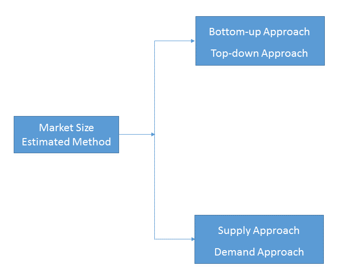
Bottom-up & top-down approach, supply & demand approach are the most important method which is used by HDIN Research to estimate the market size.
1)Top-down & Bottom-up Approach
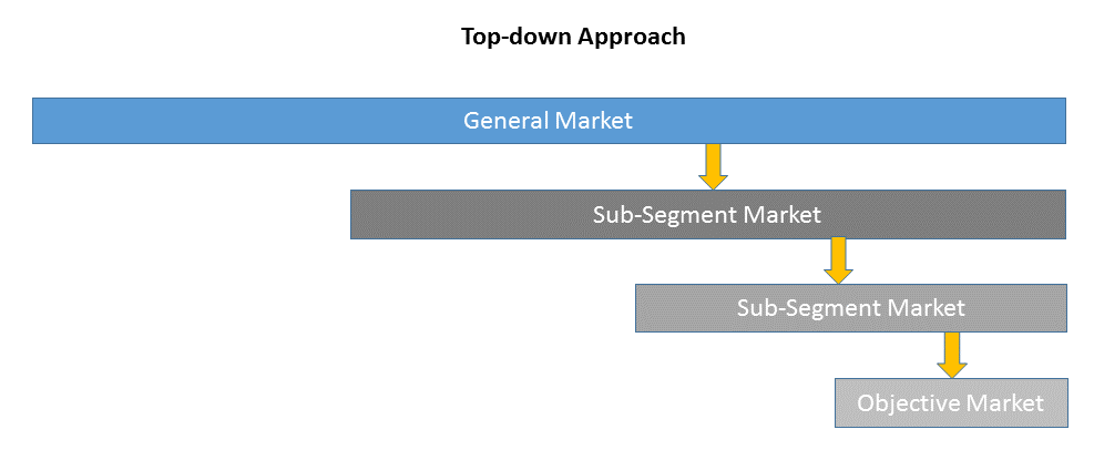
Top-down approach uses a general market size figure and determines the percentage that the objective market represents.
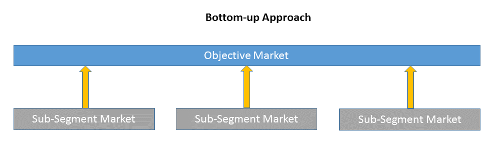
Bottom-up approach size the objective market by collecting the sub-segment information.
2)Supply & Demand Approach
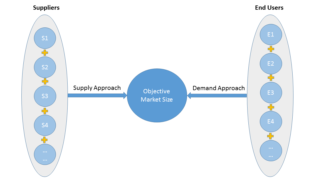
Supply approach is based on assessments of the size of each competitor supplying the objective market.
Demand approach combine end-user data within a market to estimate the objective market size. It is sometimes referred to as bottom-up approach.
- Forecasting Methodology
- Numerous factors impacting the market trend are considered for forecast model:
- New technology and application in the future;
- New project planned/under contraction;
- Global and regional underlying economic growth;
- Threatens of substitute products;
- Industry expert opinion;
- Policy and Society implication.
- Analysis Tools
1)PEST Analysis
PEST Analysis is a simple and widely used tool that helps our client analyze the Political, Economic, Socio-Cultural, and Technological changes in their business environment.
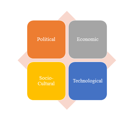
- Benefits of a PEST analysis:
- It helps you to spot business opportunities, and it gives you advanced warning of significant threats.
- It reveals the direction of change within your business environment. This helps you shape what you’re doing, so that you work with change, rather than against it.
- It helps you avoid starting projects that are likely to fail, for reasons beyond your control.
- It can help you break free of unconscious assumptions when you enter a new country, region, or market; because it helps you develop an objective view of this new environment.
2)Porter’s Five Force Model Analysis
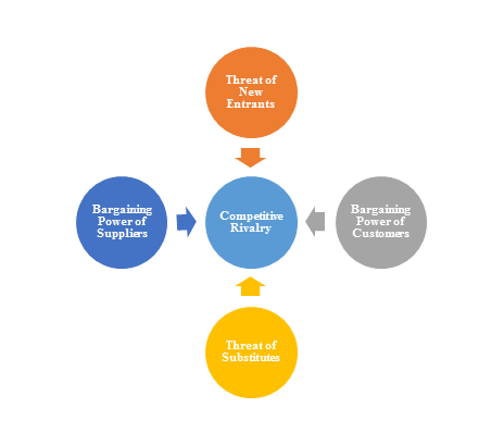
The Porter’s Five Force Model is a tool that can be used to analyze the opportunities and overall competitive advantage. The five forces that can assist in determining the competitive intensity and potential attractiveness within a specific area.
- Threat of New Entrants: Profitable industries that yield high returns will attract new firms.
- Threat of Substitutes: A substitute product uses a different technology to try to solve the same economic need.
- Bargaining Power of Customers: the ability of customers to put the firm under pressure, which also affects the customer's sensitivity to price changes.
- Bargaining Power of Suppliers: Suppliers of raw materials, components, labor, and services (such as expertise) to the firm can be a source of power over the firm when there are few substitutes.
- Competitive Rivalry: For most industries the intensity of competitive rivalry is the major determinant of the competitiveness of the industry.
3)Value Chain Analysis
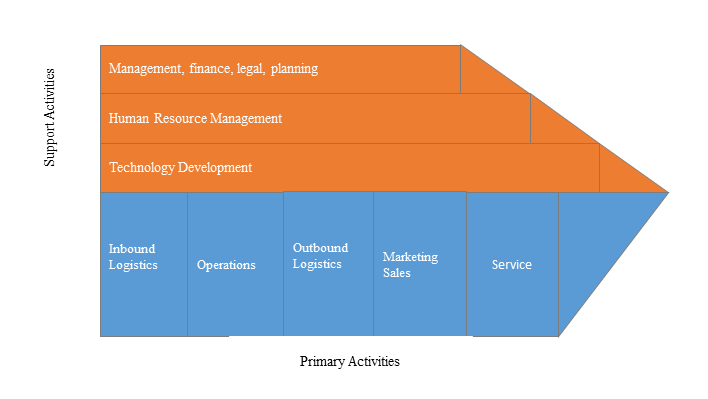
Value chain analysis is a tool to identify activities, within and around the firm and relating these activities to an assessment of competitive strength. Value chain can be analyzed by primary activities and supportive activities. Primary activities include: inbound logistics, operations, outbound logistics, marketing & sales, service. Support activities include: technology development, human resource management, management, finance, legal, planning.
4)SWOT Analysis
SWOT analysis is a tool used to evaluate a company's competitive position by identifying its strengths, weaknesses, opportunities and threats. The strengths and weakness is the inner factor; the opportunities and threats are the external factor. By analyzing the inner and external factors, the analysis can provide the detail information of the position of a player and the characteristics of the industry.
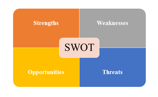
- Strengths describe what the player excels at and separates it from the competition
- Weaknesses stop the player from performing at its optimum level.
- Opportunities refer to favorable external factors that the player can use to give it a competitive advantage.
- Threats refer to factors that have the potential to harm the player.
- Data Sources
| Primary Sources | Secondary Sources |
|---|---|
| Face to face/Phone Interviews with market participants, such as: Manufactures; Distributors; End-users; Experts. Online Survey |
Government/International Organization Data: Annual Report/Presentation/Fact Book Internet Source Information Industry Association Data Free/Purchased Database Market Research Report Book/Journal/News |